


シロップタイプになっているため、これが圧倒的に飲みやすい。そして市販薬よりも副作用的な症状が出にくいのを感じています。なのでいつ使っても全然平気。それだけでも十分いいんですが、さらに効果もなかなかのもの。僕としては100点をつけてもいいレベルの商品でした。ただし飲むときは毎回数字を計る必要があるため、その点だけ唯一面倒くさい。それ以外は問題なしです。

左記クレジットカード、銀行振込、コンビニ決済に対応
左記クレジットカード、銀行振込、コンビニ決済に対応

更新日:2025/6/21
| 商品名 | デコート | クレブロス | デルタコートリル | ベポザル | ロルタジン | アレグラ | アレフェックス |
|---|---|---|---|---|---|---|---|
| 商品画像 |  |  |  |  |  |  |  |
| 特徴1 | 強力な抗炎症作用を発揮する | ・余計な作用が減弱されているので使いやすい | ・幅広い分野の治療で使用される | ・口渇や眠気の副作用が少ない | ・速効性が期待できる抗アレルギー薬 | 日本でもおなじみの抗アレルギー薬 | ・従来品の成分を改良した成分を配合 |
| 特徴2 | 喘息発作をすみやかに緩和させる | ・従来品の半量で同等の効果を発揮 | ・穏やかな作用で副腎への影響が少ない | ・速効性と持続性に優れている | ・花粉症にも高い効果を期待できる | 高用量(180mg)を選べる | ・眠気による影響を気にせずに服用できる |
| 内容量 | 0.5mg20錠x1箱 | 5mgx20錠 | 5mg20錠x1箱 | 10mg100錠x1箱 | 10mg100錠x1箱 | 120mgx20錠 | 180mg180錠x1本 |
| 価格 | 4,160円 | 4,060円 | 3,360円 | 5,860円 | 3,960円 | 3,360円 | 11,060円 |
エリアスシロップは、日本で処方される抗アレルギー薬のデザレックスと共通の有効成分(デスロラタジン)を含有しているシロップタイプの医薬品です。
錠剤を飲むのが難しい方でもスムーズに服用し、花粉症による鼻炎などを抑えることができます。
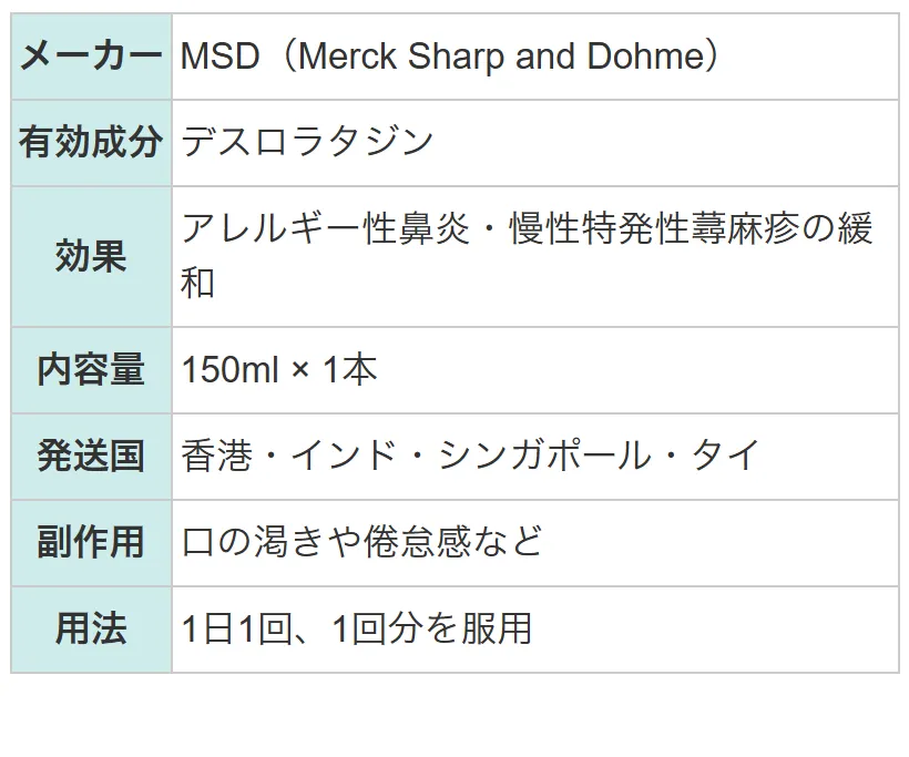
| メーカー | MSD(Merck Sharp and Dohme) |
|---|---|
| 有効成分 | デスロラタジン |
| 効果 | アレルギー性鼻炎・慢性特発性蕁麻疹の緩和 |
| 副作用 | 口の渇きや倦怠感など |
| 用法 | 1日1回、1回分を服用 |
デスロラタジンは、抗ヒスタミン作用を持つロラタジンの代謝活性物質です。体内でヒスタミン受容体に結合し、アレルギー症状の原因となるヒスタミンの行き場をなくして症状を防ぐ働きがあります。
エリアスシロップには、150ml中にデスロラタジン0.5mg/mlを含有しています。

| 個数 | 販売価格(1本あたり) | 販売価格(箱) | ポイント | 購入 |
|---|---|---|---|---|
| 1本 | 4,860円 | 4,860円 | 145pt | 売り切れ |
| 3本 | 2,753円 | 8,260円 | 247pt | 売り切れ |
| 5本 | 2,312円 | 11,560円 | 346pt | 売り切れ |


①1万円以上で送料無料
1回の注文で10,000円以上だった場合、1,000円の送料が無料となります。
まとめ買いをすると1商品あたりのコストパフォーマンスが高くなるためおすすめです。
②プライバシー守る安心梱包
外箱に当サイト名や商品名が記載されることはないため、ご家族や配達員など第三者に内容を知られることは御座いません。

③100%メーカー正規品取り扱い
当サイトの商品は100%メーカー正規品となっており、第三者機関による鑑定も行っております。
商品の破損などがあった場合は再配送などにて対応させて頂きますので、ご連絡頂ければ幸いです。

④いつでも購入可能 処方箋不要
サイト上では24時間いつでもご注文を受けております。
また、お電話によるご注文も受け付けておりますのでネットが苦手な方はお気軽にどうぞ。

⑤商品到着100%
商品発送後はお荷物の追跡状況が分かる追跡番号をご案内させて頂きます。
郵便局には保管期限がありますのでご注意ください。
・自宅配達で不在だった場合の保管期限・・・16日間前後
・郵便局留めとした場合の保管期限・・・7~30日間

⑥コンビニ決済利用可能
ご近所のコンビニにていつでもお支払可能です。
セブンイレブンに限り店舗での機械操作を必要とせず、手続き完了後に表示されるバーコードや払込票番号をレジに提示することでお支払い頂けます。

エリアスシロップ 150ml x 5本
11,560円
ポイント:346pt
10,000円以上購入で送料無料
売り切れ

シロップタイプになっているため、これが圧倒的に飲みやすい。そして市販薬よりも副作用的な症状が出にくいのを感じています。なのでいつ使っても全然平気。それだけでも十分いいんですが、さらに効果もなかなかのもの。僕としては100点をつけてもいいレベルの商品でした。ただし飲むときは毎回数字を計る必要があるため、その点だけ唯一面倒くさい。それ以外は問題なしです。
シロップタイプになっているので飲みやすさは全然いいんですが、効き目は思っていたより低かったです。飲んでしばらくしてからも鼻づまりはあまり改善されませんし、咳なども出てしまっています。ただ、症状が弱い兄弟が飲んだらけっこう効いたみたいなので症状がかなり弱い人が飲んだらいいのかもしれません。私みたいなけっこう重症になっている方には向いていません。
服用するお薬の種類によります。ステロイド系のお薬だと長期服用は副作用が現れやすくなるため短期間に留めてください。抗アレルギー薬であれば3~4ヶ月ほどはほぼ問題なく継続服用することが可能です。
眠気などの副作用が強く現れるおそれがあるため原則控えてください。どうしてもお酒を飲みたい、または飲まなければいけない場合は飲酒から3~4時間を空けてお薬を服用してください。(あくまで目安です。飲酒量が多い場合は更に多くの時間を要します。)
同じ、または近い作用を持つお薬の併用は控えてください。併用により副作用がより強く現われたり、予想しない症状が現れる場合があります。稀に医師の判断で抗ヒスタミン剤が複数処方されることがありますが、適切な指導がない状況での併用は控えましょう。
アレルギー薬に多い抗ヒスタミン薬には眠気の副作用があるため、運転や高所での作業などは控えましょう。運転を行う日などは服用しない、または漢方薬のような眠くなる成分を含まない対策を用意してくことを推奨いたします。
症状に合わせた目薬を使用することを推奨いたします。特にステロイド点眼薬は炎症を鎮める効果が高い反面、副作用が現れやすいため使用回数や期間には注意が必要です。そのため普段使いには非常に不向きです。
原則的に妊娠4ヶ月半まではお薬の使用を避けるべきとされています。どうしても症状が辛い場合はまずは医師に相談することを推奨いたします。医師への相談なく市販のアレルギー薬を使用するといったことは控えましょう。
口の乾きは眠気と同様にアレルギー薬に多く見られる副作用です。基本的に危険な副作用ではないですが症状がどうしても気になるようであれば、医師に相談することを推奨いたします。
| 1日の服用回数 | 1回 |
|---|---|
| 1回の服用量 | 10ml |
| 服用のタイミング | アレルギー症状などが出ている期間 |
| 服用期間 | 24時間 |
| 2%未満 | 頻度不明 | |
| 神経系障害 | 傾眠 | 頭痛、精神運動亢進 |
| 心臓障害 | 頻脈、動悸 | |
| 胃腸障害 | 口内乾燥 | |
| 皮膚及び皮下組織障害 | 発疹 | |
| 一般・全身障害及び投与部位の状態 | 疲労 | |
| その他 | 白血球数増加、血中コレステロール増加 | 食欲亢進 |
本製品は海外製のため、期限表記が日本と異なる場合がございます。
パッケージ裏面や側面、シートなどに以下のような表記がされています。
| EXP | 使用期限 例:EXP 12/2025→2025年12月まで使用可 |
|---|---|
| MFG または MFD | 製造日 例:MFG 03/2023 |
| BEST BEFORE | 品質が最も安定している目安日 |
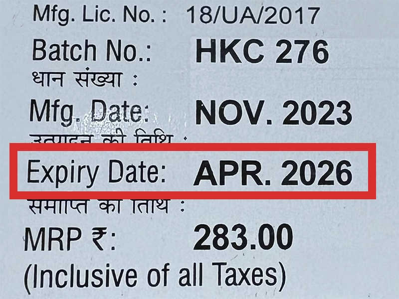
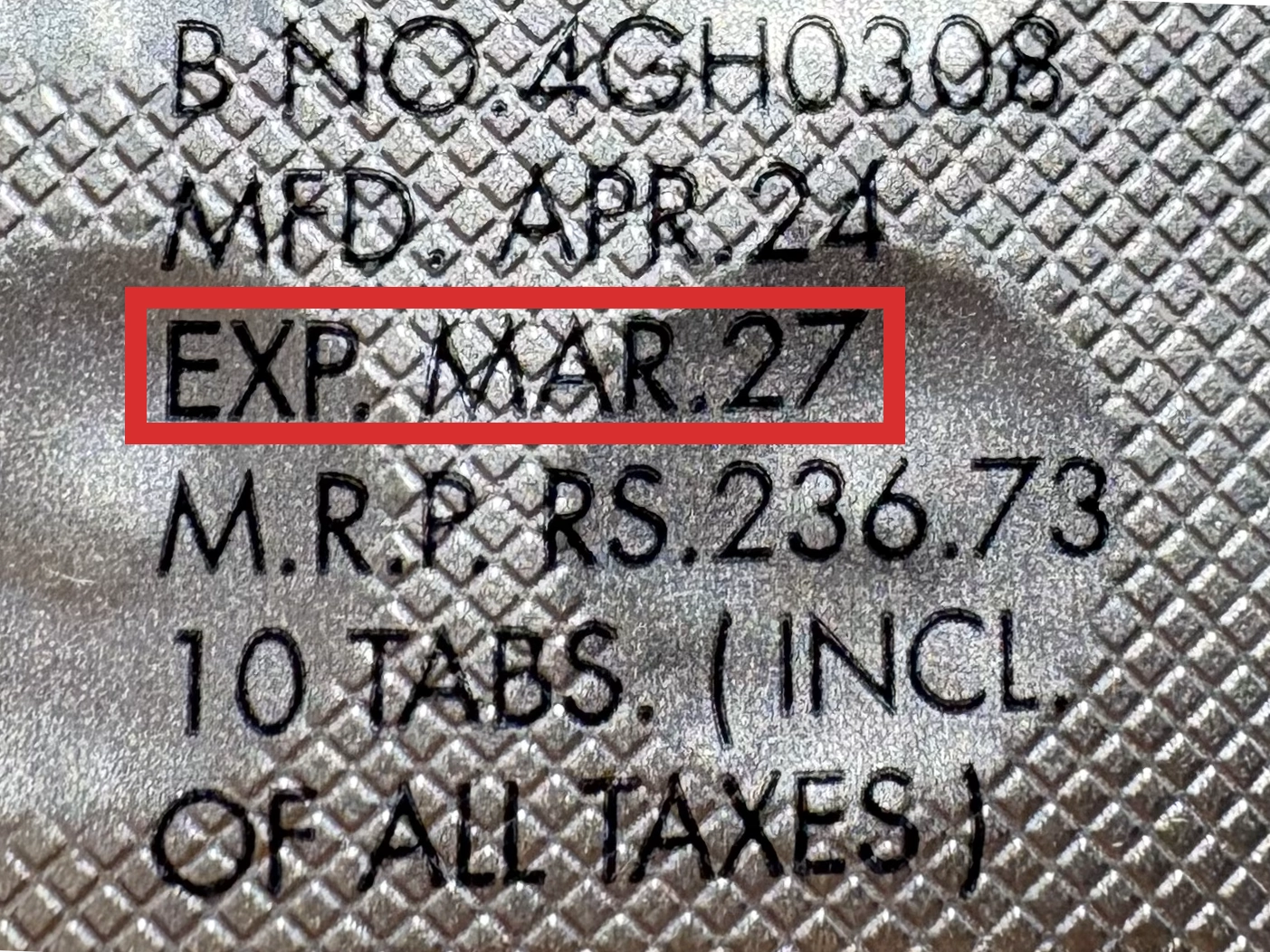
※国や製品により日付の並び(例:月/年、日/月/年)が異なる場合がありますのでご注意ください
EXP(Expiry Date) の表記がなく、MFG または MFDしか記載がないケースがあります。
この場合は MFG(MFD) から2~3年が使用期限の目安です。
※「LOT」や「BATCH」の表記は製造番号であり期限ではありません。

パッケージ例となります。
商品やご注文単位によってはシート単位でのお届けとなる場合が御座います。
外箱に当サイト名や商品名が記載されることはないため、ご家族や配達員など第三者に内容を知られることは御座いません。
錠剤よりもさらに飲みやすいアレルギー薬を探していたら、これを発見しました!飲む際に計量しないといけないのは面倒ですが、錠剤のアレルギー薬よりも早く飲めて、忙しい日はとても便利です。
シロップタイプになっているため、これが圧倒的に飲みやすい。そして市販薬よりも副作用的な症状が出にくいのを感じています。なのでいつ使っても全然平気。それだけでも十分いいんですが、さらに効果もなかなかのもの。僕としては100点をつけてもいいレベルの商品でした。ただし飲むときは毎回数字を計る必要があるため、その点だけ唯一面倒くさい。それ以外は問題なしです。
薬が苦手な子ども用に買ったんですが、子どもは錠剤を飲みこなせるようになり、シロップをすぐ卒業しました。子どもいわく、シロップは計量しないといけないのが面倒とのことでした。子どもが飲まなくなって、逆に私がシロップタイプをよく使うようになりました。なんとなく錠剤よりも効き目が強い気がして、飲み切った後に追加でもう一本買ってしまいました。すっかり私用の薬です。
夫がシロップタイプを使いたいと言ってこちらを購入してました。子どもじゃあるまいし錠剤も飲めてたじゃん…と何度か言いました。が、一度使い始めたらなかなか戻りたくなくなるとのことだったので、気になって自分でも使ってみたら、確かに戻りたくなくなる気持ちわかりました笑 これで一ヶ月ぐらい使えるのは許容範囲かと。でもわざわざ買うのは面倒だし、二人分をまとめ買いします。
一年を通して鼻炎が続いてるような体質なので、アレルギー性の薬を飲んだ方がいいのはわかっているんですけど、私が薬嫌いという理由で飲んでません。それでも「この時期はしんどいな」と感じる時期に入ると、仕方なく飲んでます。できるだけ飲む時に楽をしたいので、エリアスシロップをたびたび活用してます。スーッと飲めるので楽です。効き目は錠剤と何も変わらないです。
商品口コミの投稿は会員のみ行えるようになっております。
お手数ですが会員ログインの上でご投稿頂きますようお願いいたします。
口コミをご投稿頂いたお客様にはポイントをプレゼントさせて頂いております。
文章のみであれば100ポイント、文章+写真付きのものは300ポイントをプレゼントさせて頂きます。
規約や詳細などはこちらをご確認くださいませ。