


病気をテーマにしたテレビ番組を見ていると、いてもたってもいられなくなってちょっと良い薬を使おうと思いました。この商品は高脂血症に良いとされているみたいなので、これで重たい病気をしないようしっかりカバーしていきたいと思います。

左記クレジットカード、銀行振込、コンビニ決済に対応
左記クレジットカード、銀行振込、コンビニ決済に対応


更新日:2025/6/13
ノルバスクは、有効成分アムロジペンペシル酸塩の先発医薬品で、世界的な製薬メーカーのファイザー(Pfizer)が製造を手がけています。
ゆるやかに血圧を下げることで高血圧の症状を改善させ、狭心症発作を予防する効果も発揮します。
| メーカー | ファイザー(Pfizer) ヴィアトリス(Viatris) |
|---|---|
| 有効成分 | アムロジピンべシル酸塩 |
| 効果 | 高血圧症の改善 狭心症の発作予防 |
| 副作用 | 浮腫や頭痛など |
| 用法 | 1日1回、1回分を服用 |
アムロジピンべシル酸塩には、細胞膜のカルシウムチャネル(カルシウムイオンの流入経路)を遮断する作用があります。カルシウムイオンは血管平滑筋の収縮に深く関わっているため、流入経路が遮断されることで収縮が緩み、弛緩することになります。結果的に血管が拡張し、血圧が下がる仕組みです。
ノルバスクには、1錠あたりの配合量が異なる5mg錠、10mg錠の2種類があります。

| 個数 | 販売価格(1錠あたり) | 販売価格(箱) | ポイント | 購入 |
|---|---|---|---|---|
| 30錠 | 138円 | 4,160円 | 124pt | |
| 60錠 | 92円 | 5,560円 | 166pt |
| 個数 | 販売価格(1錠あたり) | 販売価格(箱) | ポイント | 購入 |
|---|---|---|---|---|
| 30錠 | 172円 | 5,160円 | 154pt |


①1万円以上で送料無料
1回の注文で10,000円以上だった場合、1,000円の送料が無料となります。
まとめ買いをすると1商品あたりのコストパフォーマンスが高くなるためおすすめです。
②プライバシー守る安心梱包
外箱に当サイト名や商品名が記載されることはないため、ご家族や配達員など第三者に内容を知られることは御座いません。

③100%メーカー正規品取り扱い
当サイトの商品は100%メーカー正規品となっており、第三者機関による鑑定も行っております。
商品の破損などがあった場合は再配送などにて対応させて頂きますので、ご連絡頂ければ幸いです。

④いつでも購入可能 処方箋不要
サイト上では24時間いつでもご注文を受けております。
また、お電話によるご注文も受け付けておりますのでネットが苦手な方はお気軽にどうぞ。

⑤商品到着100%
商品発送後はお荷物の追跡状況が分かる追跡番号をご案内させて頂きます。
郵便局には保管期限がありますのでご注意ください。
・自宅配達で不在だった場合の保管期限・・・16日間前後
・郵便局留めとした場合の保管期限・・・7~30日間

⑥コンビニ決済利用可能
ご近所のコンビニにていつでもお支払可能です。
セブンイレブンに限り店舗での機械操作を必要とせず、手続き完了後に表示されるバーコードや払込票番号をレジに提示することでお支払い頂けます。

ノルバスク 5mg x 30錠
4,160円
ポイント:124pt
10,000円以上購入で送料無料
在庫あり

病気をテーマにしたテレビ番組を見ていると、いてもたってもいられなくなってちょっと良い薬を使おうと思いました。この商品は高脂血症に良いとされているみたいなので、これで重たい病気をしないようしっかりカバーしていきたいと思います。
血圧高めだったのでノルバスクを購入して飲んでいましたが、血圧が下がるような感じはまるでありません。逆に上がっていることもあるくらいです。私は60錠タイプのものを購入しており、すでに1ヶ月半以上飲んでいるんですが、未だに結果を出すことができていません。このままだと血圧が下がることなく飲み終わることになりそうです。少しでも効いてくれればよかったのですが...
ノルバスクは血管の筋肉をゆるめて血の流れをスムーズにし、血圧を下げる薬です。特に末梢の血管の抵抗を減らすことで、心臓への負担も軽くなります。作用はゆっくり始まり、長く続くのが特徴です。
ノルバスクは心臓の血管を広げ、血の流れをよくして酸素不足を解消し、狭心症の発作を減らします。胸の痛みの改善や発作予防に使われることも多い薬です。
ノルバスクはゆっくりと効果を発揮し、長く続くのが特徴です。急な効果は期待できませんが、毎日続けることで安定した降圧や狭心症の予防が可能です。
ノルバスクは1日1回の服用でも、約24時間にわたって安定した効果が続きます。毎日同じ時間に飲むことで、血圧や症状のコントロールがしやすくなります。
1日1回の服用が基本です。高血圧症では2.5〜5mgから始め、効果が不十分な場合は10mgまで増量することがあります。毎日同じ時間に飲むことで、安定した効果が得られます。
長期間服用に対する安全性は確認されています。高血圧や狭心症の安定した管理のためにも、適切に服用を継続することが重要です。
自己判断での中断はせず、継続するようにしてください。血圧が正常になってきても高血圧や狭心症は慢性的に進行することがあるため、医師と相談しながら継続や中止などを決めるようにしてください。
関係ありません。ノルバスクは食事による影響がほとんどないため、食前でも食後でも服用できます。ですが、飲み忘れを防止するために食前や食後などを決めて服用する方はいらっしゃいます。
劇症肝炎や無顆粒球症、白血球減少などが報告されています。全身のだるさや筋肉痛、尿の色が濃くなるなどの症状が出た場合、早急に医療機関を受診するようにしてください。
特定の薬との併用で副作用リスクが高まったり、効果が弱まったりすることがあります。併用に注意が必要な薬として、グレープフルーツジュースやシンバスタチンなどがあります。飲み合わせには注意し、事前に問題がないか確認するようにしてください。
ノルバスクの副作用として足のむくみ(浮腫)が比較的多く見られます。特に高い用量を服用している場合に起こりやすいとされています。一時的なものであれば問題ありませんが、長く副作用が続くような場合は医師に相談するようにしましょう。
めまいやむくみ、頭痛や動悸、顔のほてりなどが比較的よく見られます。これらは一時的なことが多いですが、長引く場合は医師に相談してください。また、これら以外にもさまざまな副作用の報告はあるので、十分に注意しましょう。
| 1日の服用回数 | 1回 |
|---|---|
| 1回の服用量 | 2.5~5mg |
| 服用のタイミング | 指定なし |
| 服用期間 | 24時間以上 |
| 1日の服用回数 | 1回 |
|---|---|
| 1回の服用量 | 5mg |
| 服用のタイミング | 指定なし |
| 服用期間 | 24時間以上 |
| 商品名 | メインテート・ジェネリック | アムロジス | イプシトロン | アテレックジェネリック | セレペグ | テルマヒール40-AM | ペリンドプリルエルブミン |
|---|---|---|---|---|---|---|---|
| 商品画像 |  |  |  |  |  |  |  |
| 特徴1 | ・大容量で低価格なので長期服用に最適 | ・1日1回の服用で効果が持続 | ・効果と安全性が高いACE阻害薬 | ・合併症が多い高齢者の方にも適している | ・ウプトラビと同一成分のジェネリック | ・2つの成分が効果的に血圧を下げる降圧薬 | ・血圧を上げる物質の生成を抑える |
| 特徴2 | ・安全性と持続性に優れている | ・血流改善によって様々な疾患に有効 | ・心臓や腎臓の負担も軽減できる | ・効果と安全性が高く、信頼性も十分にある | ・1回の服用で長時間効果が持続 | ・長時間型なので長い効果が期待できる | ・心臓や腎臓の負担を軽くする |
| 内容量 | 5mgx100錠 | 10mg20錠x1箱 | 25mg100錠x1箱 | 5mg150錠x1箱 | 200mcg10錠x1箱 | 150錠x1箱 | 4mg30錠x1箱 |
| 価格 | 3,160円 | 4,960円 | 4,960円 | 5,760円 | 4,960円 | 9,800円 | 4,160円 |
| 0.1〜1%未満 | 0.1%未満 | 頻度不明 | |
| 肝臓 | ALT、ASTの上昇、肝機能障害、ALP、LDHの上昇 | γ-GTP上昇、黄疸 | 腹水 |
| 循環器 | 浮腫注1)、ほてり(熱感、顔面潮紅等)、動悸、血圧低下 | 胸痛、期外収縮、洞房又は房室ブロック、洞停止、心房細動、失神、頻脈 | 徐脈 |
| 精神・神経系 | めまい・ふらつき、頭痛・頭重 | 眠気、振戦、末梢神経障害 | 気分動揺、不眠、錐体外路症状 |
| 消化器 | 心窩部痛、便秘、嘔気・嘔吐 | 口渇、消化不良、下痢・軟便、排便回数増加、口内炎、腹部膨満、胃腸炎 | 膵炎 |
| 筋・骨格系 | 筋緊張亢進、筋痙攣、背痛 | 関節痛、筋肉痛 | |
| 泌尿・生殖器 | BUN上昇 | クレアチニン上昇、頻尿・夜間頻尿、尿管結石、尿潜血陽性、尿中蛋白陽性 | 勃起障害、排尿障害 |
| 代謝異常 | 血清コレステロール上昇、CK上昇、高血糖、糖尿病、尿中ブドウ糖陽性 | ||
| 血液 | 赤血球、ヘモグロビン、白血球の減少、白血球増加、紫斑 | 血小板減少 | |
| 過敏症 | 発疹 | そう痒、じん麻疹、光線過敏症 | 多形紅斑、血管炎、血管浮腫 |
| 口腔 | (連用により)歯肉肥厚 | ||
| その他 | 全身倦怠感 | しびれ、脱力感、耳鳴、鼻出血、味覚異常、疲労、咳、発熱、視力異常、呼吸困難、異常感覚、多汗、血中カリウム減少 | 女性化乳房、脱毛、鼻炎、体重増加、体重減少、疼痛、皮膚変色 |
本製品は海外製のため、期限表記が日本と異なる場合がございます。
パッケージ裏面や側面、シートなどに以下のような表記がされています。
| EXP | 使用期限 例:EXP 12/2025→2025年12月まで使用可 |
|---|---|
| MFG または MFD | 製造日 例:MFG 03/2023 |
| BEST BEFORE | 品質が最も安定している目安日 |
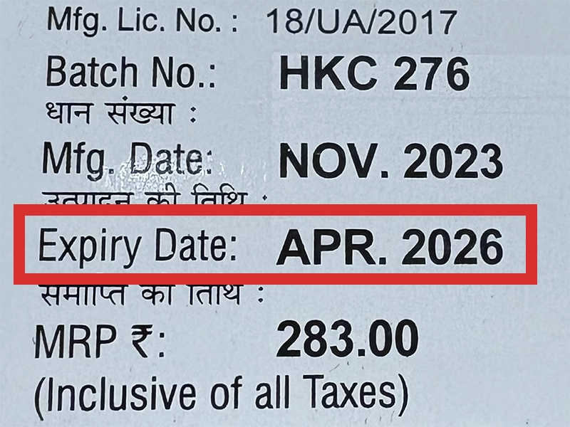
※国や製品により日付の並び(例:月/年、日/月/年)が異なる場合がありますのでご注意ください
EXP(Expiry Date) の表記がなく、MFG または MFDしか記載がないケースがあります。
この場合は MFG(MFD) から2~3年が使用期限の目安です。
※「LOT」や「BATCH」の表記は製造番号であり期限ではありません。

パッケージ例となります。
商品やご注文単位によってはシート単位でのお届けとなる場合が御座います。
外箱に当サイト名や商品名が記載されることはないため、ご家族や配達員など第三者に内容を知られることは御座いません。
病気をテーマにしたテレビ番組を見ていると、いてもたってもいられなくなってちょっと良い薬を使おうと思いました。この商品は高脂血症に良いとされているみたいなので、これで重たい病気をしないようしっかりカバーしていきたいと思います。
しばらく飲んでいますが、なかなか血圧が安定して下がってくれないですね。私は飲み始めてから数か月は経過するのですが、飲み始めと比べてもプラスマイナス5くらいしか変わらないです。塩分とかアルコールの量には気を付けているはずなのですが。このまま特に何も変わらないのなら他の医薬品に変えるか、医師に相談して適した医薬品をしょうかいしてもらおうと思います。
若い時は特に異常はなかったのに40代から高血圧気味になりました。おかげで好きなものをたくさん食べたり、お酒を飲んだりする量を減らしました。それでもあまり数値が下がらなかったので、医薬品の力を頼りたいと思いノルバスクを飲んでいます。すると、少しずつ血圧が下がるようになりました。副作用とかが怖くて医薬品は飲みたくなかったのですが最初から飲んでおけばと思いました。
病院で受けた健康診断で血圧に注意といわれ、それ以来自分でも気を付けるようにしてきました。でも、血圧測定器で測ると高い数値のままでした。このままじゃまずいと思い、ノルバスクを最近飲み始めました。まだ、数回しか飲んでいないのですが次の日に測ってみると、わずかに血圧が下がっていました。少しでも下がっていれば飲み続ける価値はあると思うのでしばらくは飲んでおきます。
若い時からお酒と脂っこい食事が好きで、ついつい飲み食いしていました。すると、40代で高血圧や糖尿病の予備軍になってしまいました。このままじゃ美味しいものを食べる前に死んでしまうと思い、このノルバスクを買いました。服用している間はお酒も脂っこい食事も頑張って控えました。その後、自分で買った血圧測定器で測るとかなり血圧が下がっていました!
商品口コミの投稿は会員のみ行えるようになっております。
お手数ですが会員ログインの上でご投稿頂きますようお願いいたします。
口コミをご投稿頂いたお客様にはポイントをプレゼントさせて頂いております。
文章のみであれば100ポイント、文章+写真付きのものは300ポイントをプレゼントさせて頂きます。
規約や詳細などはこちらをご確認くださいませ。