


これは、凄い!わざわざ病院に行かなくても手に入るのが凄い!ちゃんと効き目もあるのが凄い!自分は昔から心臓があまりよろしくないし血圧もあまりよろしくないのだが、そんな自分にはぴったりの薬と感じる。前に別の薬を飲んでいたときはあんまり体に合わなかったりしたこともあるのだが、ベタックは自分の体に合っているのがわかる。

左記クレジットカード、銀行振込、コンビニ決済に対応
左記クレジットカード、銀行振込、コンビニ決済に対応


更新日:2025/6/19
| 商品名 | リオシ | オルメタイム | ジルゼム | ハイザール | ノルバスクジェネリック | フェロ | エナラプリル+レルカニジピン |
|---|---|---|---|---|---|---|---|
| 商品画像 |  |  |  |  |  |  |  |
| 特徴1 | ・肺高血圧症治療薬アデムパスのジェネリック | ・2つの有効成分で高い効果が期待できる | ・効果と安全性が高いカルシウム拮抗薬 | ・ジェネリックだから安価で治療できる | 1回の服用で24時間効果が持続する | ・有効性と安全性に優れた高血圧治療薬 | ・2種類の降圧剤を配合 |
| 特徴2 | ・血管拡張作用で息切れや疲労感を軽減 | ・比較的副作用が少ない降圧剤 | ・全身の血流を改善 | ・ふたつの成分が効果的に血圧を下げる | 安価に購入できるジェネリック | ・効き目が強く、副作用の少ない | ・有名製薬会社マイランのジェネリック医薬品 |
| 内容量 | 1mg100錠x1箱 | 30錠x1箱 | 30mg100錠x1箱 | 50mg/12.5mgx28錠 | 10mgx30錠 | 5ER5mg90錠x1箱 | 10mg+10mg 56錠x1箱 |
| 価格 | 9,360円 | 4,060円 | 4,360円 | 4,060円 | 2,800円 | 4,500円 | 4,160円 |

| 個数 | 販売価格(1錠あたり) | 販売価格(箱) | ポイント | 購入 |
|---|---|---|---|---|
| 30錠 | 135円 | 4,060円 | 121pt | 売り切れ |
| 60錠 | 86円 | 5,160円 | 154pt | 売り切れ |
| 90錠 | 69円 | 6,260円 | 187pt | 売り切れ |


①1万円以上で送料無料
1回の注文で10,000円以上だった場合、1,000円の送料が無料となります。
まとめ買いをすると1商品あたりのコストパフォーマンスが高くなるためおすすめです。
②プライバシー守る安心梱包
外箱に当サイト名や商品名が記載されることはないため、ご家族や配達員など第三者に内容を知られることは御座いません。

③100%メーカー正規品取り扱い
当サイトの商品は100%メーカー正規品となっており、第三者機関による鑑定も行っております。
商品の破損などがあった場合は再配送などにて対応させて頂きますので、ご連絡頂ければ幸いです。

④いつでも購入可能 処方箋不要
サイト上では24時間いつでもご注文を受けております。
また、お電話によるご注文も受け付けておりますのでネットが苦手な方はお気軽にどうぞ。

⑤商品到着100%
商品発送後はお荷物の追跡状況が分かる追跡番号をご案内させて頂きます。
郵便局には保管期限がありますのでご注意ください。
・自宅配達で不在だった場合の保管期限・・・16日間前後
・郵便局留めとした場合の保管期限・・・7~30日間

⑥コンビニ決済利用可能
ご近所のコンビニにていつでもお支払可能です。
セブンイレブンに限り店舗での機械操作を必要とせず、手続き完了後に表示されるバーコードや払込票番号をレジに提示することでお支払い頂けます。

ベタック 10mg x 90錠
6,260円
ポイント:187pt
10,000円以上購入で送料無料
売り切れ

これは、凄い!わざわざ病院に行かなくても手に入るのが凄い!ちゃんと効き目もあるのが凄い!自分は昔から心臓があまりよろしくないし血圧もあまりよろしくないのだが、そんな自分にはぴったりの薬と感じる。前に別の薬を飲んでいたときはあんまり体に合わなかったりしたこともあるのだが、ベタックは自分の体に合っているのがわかる。
血圧は確かに下がるんですけど、薬との相性が悪いのかちょっと効きすぎ?な感じがして、あまり合わなかったので個人的には星2つですね。
高血圧や狭心症の治療に使われる薬です。心臓のはたらきをやさしく抑えて、血圧を下げたり、胸の痛みを防いだりします。特に「腎臓が悪くて血圧が高くなっている人」にも使われることがありますが、基本的には高血圧の薬として広く使われています。
心臓の負担を減らすことで狭心症の発作を防ぐ効果があります。心筋の酸素消費量を減らし、運動中の胸の痛みを軽減します。発作の回数が減るだけでなく、運動できる時間が延びるなど、日常生活の質を上げる効果も期待できます。
飲み始めてから数日以内にじわじわと血圧が下がり始めます。効果が安定するまでは1週間ほどかかることもありますが、1日1回の服用で24時間しっかり効くので、続けることで安定した降圧効果が期待できます。
52週間の長期使用試験でも、約8割の患者で安定した効果が続いたと報告されています。副作用の発現も少なく、長期的に安心して使える薬とされています。しっかり続けることで、血圧コントロールが安定しやすくなります。
気づいた時点ですぐに1回分を飲んでください。ただし、次に飲む時間が近い場合は、1回分を飛ばしてもかまいません。2回分をまとめて飲むのは危険なので絶対にやめましょう。飲み忘れが続く場合は、医師に相談してください。
毎日、朝の同じ時間に1日1回飲むのが基本です。ベタキソロールは長く効くタイプの薬で、1回飲めば1日中安定して効果が続きます。毎回決まった時間に飲むことで、血圧の変動が少なくなり、飲み忘れも防ぎやすくなります。
はい、朝食を抜いた日でも薬はいつも通り飲んでかまいません。この薬は食事の有無にかかわらず効果がしっかり出ます。ただし、空腹時に飲むと気分が悪くなる人もいるので、体調に合わせてタイミングを調整するのも一つの方法です。
ベタックを気づける場所に置くのがポイントです。たとえば冷蔵庫、歯ブラシの横、玄関など、自分が毎日必ず見る場所に置くと飲み忘れにくくなります。スマホのアラームやアプリを使うのも便利です。
はい。特に心拍をさらに下げる薬(カルシウム拮抗薬など)や、血圧を下げる薬との併用には注意が必要です。眠気やふらつきが強くなることがあります。市販薬やサプリでも相互作用があるものがあるので、新しく飲む前には必ず確認してください。
血圧が下がることで、一時的にめまいやふらつきが出ることがあります。特に薬を飲み始めた最初の数日間や、立ち上がった瞬間などに起こりやすいです。急に立ち上がらず、ゆっくり動くようにしましょう。症状が強いときは医師に相談してください。
妊娠中は、胎児への影響の可能性があるため使用を避けるべきです。授乳中も母乳に移行する可能性があるとされており、慎重な判断が必要です。妊娠の可能性がある方や、妊活中の方は事前に医師へ必ず伝えてください。
心拍数や血圧が低めに出ることがあります。とくに運動負荷をかけるような検査では、心拍数が上がりにくくなることで「反応が鈍い」と判断されることもあります。健康診断などではあらかじめ、薬を服用してもいいか確認したり、この薬を飲んでいますと伝えておくようにしましょう。
| 1日の服用回数 | 1回 |
|---|---|
| 1回の服用量 | 5~10mg |
| 服用のタイミング | 指定なし |
| 服用間隔 | 指定なし |
| 0.1〜5%未満 | 0.1%未満 | 頻度不明 | |
| 循環器 | 徐脈 | 動悸、胸痛 | レイノー現象、洞停止、低血圧、心電図異常、房室ブロック |
| 眼 | 目のちらつき | 涙液分泌減少、霧視(感) | |
| 過敏症 | 蕁麻疹、そう痒 | 発疹 | |
| 精神神経系 | ふらふら感、頭痛、めまい、ぼんやり、眠気、不眠 | 幻覚、悪夢、蟻走感 | うつ状態 |
| 消化器 | 下痢、口渇、悪心、胃部不快感 | 胃痛、嘔吐 | |
| 肝臓 | 肝機能障害(AST、ALT、Al-P、γ-GTP、LDH上昇等) | ||
| 呼吸器 | 呼吸困難 | 喘息症状 | |
| 腎臓 | BUN上昇 | ||
| その他 | 倦怠感、疲労感、しびれ感 | 耳鳴、熱感、発汗、浮腫 | 尿酸値上昇、中性脂肪上昇、コレステロール上昇、高血糖、CK上昇、HDL-コレステロール低下、脱力感、インポテンス |
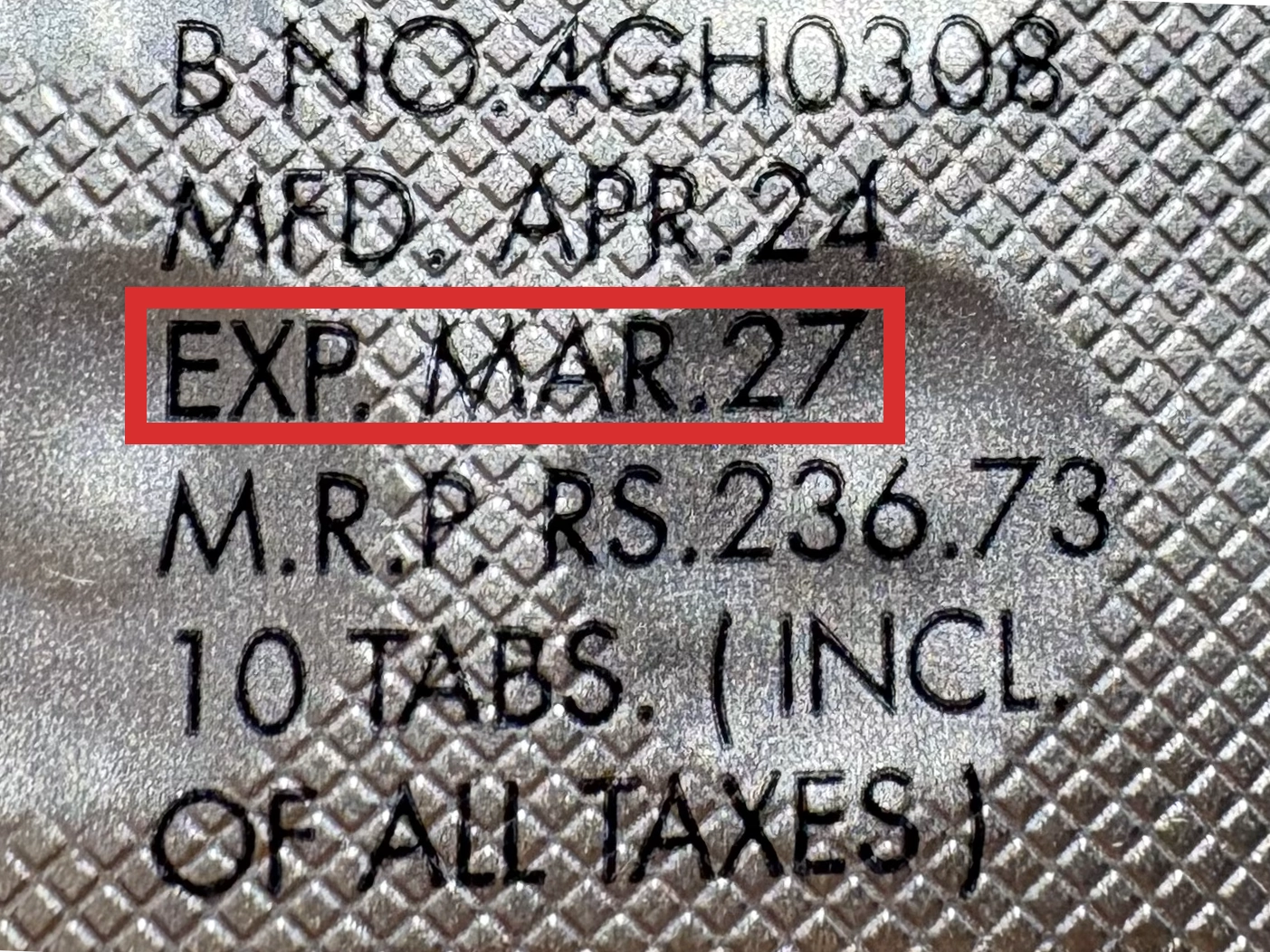
本製品は海外製のため、期限表記が日本と異なる場合がございます。
パッケージ裏面や側面、シートなどに以下のような表記がされています。
| EXP | 使用期限 例:EXP 12/2025→2025年12月まで使用可 |
|---|---|
| MFG または MFD | 製造日 例:MFG 03/2023 |
| BEST BEFORE | 品質が最も安定している目安日 |
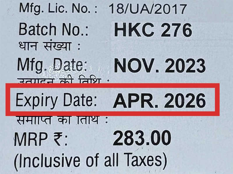
※国や製品により日付の並び(例:月/年、日/月/年)が異なる場合がありますのでご注意ください
EXP(Expiry Date) の表記がなく、MFG または MFDしか記載がないケースがあります。
この場合は MFG(MFD) から2~3年が使用期限の目安です。
※「LOT」や「BATCH」の表記は製造番号であり期限ではありません。

パッケージ例となります。
商品やご注文単位によってはシート単位でのお届けとなる場合が御座います。
外箱に当サイト名や商品名が記載されることはないため、ご家族や配達員など第三者に内容を知られることは御座いません。
これは、凄い!わざわざ病院に行かなくても手に入るのが凄い!ちゃんと効き目もあるのが凄い!自分は昔から心臓があまりよろしくないし血圧もあまりよろしくないのだが、そんな自分にはぴったりの薬と感じる。前に別の薬を飲んでいたときはあんまり体に合わなかったりしたこともあるのだが、ベタックは自分の体に合っているのがわかる。
ベタックは、それなりに良い薬だと思っていいのではないかと思います。ちょっとフラッとしたんだけど副作用らしいし、2日目からは何もなくて健康に服用を続けることができています。次回の健康診断で良い結果がでたらいいなと思っています。
高血圧のケがあるから、不安なので薬をのむ事にして、いくつか吟味して買ったのがベタック。飲んでみた感じ体には合っていそう。このまま数値が下がってくれればいいのですが、とにかく飲んだ感じが良かったので、ひとまず星を五つつけましたが、今後どうなるかは数値次第というところでしょう。ちなみに体調は特に変わったところはありません。海外の薬なので副作用は心配でしたが、今の所なにもないようです。
糖尿と高血圧で二か月に1回、病院で検査してもらってお薬を処方してもらってましたが、仕事が忙しくなり通院も難しくなってきたので、通販サイトで買うようになりました。最初は病院で処方されているのと同じケルロングを買ってましたが、ジェネリックのベタックがあるのを知ってからはそちらを買ってます。効果はケルロングと変わらないです。毎日服用して血圧が高くなりすぎないよう維持できています。
フランスで料理人として働いていた時に体調を崩して不整脈になってしまい。ベタックを服用していました。日本に帰国して病院で別の薬を処方してもらいましたが、副作用が出る等合わなくて、どうしようかと思っていたら、日本でも個人輸入でベタックを購入できると知って、ココロ薬局さんで買うようになりました。血圧も下がってくれますし、日本でも料理人として再び働けるようになりました。
商品口コミの投稿は会員のみ行えるようになっております。
お手数ですが会員ログインの上でご投稿頂きますようお願いいたします。
口コミをご投稿頂いたお客様にはポイントをプレゼントさせて頂いております。
文章のみであれば100ポイント、文章+写真付きのものは300ポイントをプレゼントさせて頂きます。
規約や詳細などはこちらをご確認くださいませ。