


心臓に圧迫感のある痛みというか苦しさを感じてコンコールを使ってみました。今までに経験したことのないような痛みと場所が場所なだけにかなり焦りました。焦ると余計に痛くなるような気がしたのでできるだけ自分を落ち着かせるためにも薬は有効的でした。今ではほとんど痛くなることがなくなったので薬の回数を減らしたり痛いときにだけ飲むようにして副作用の影響を減らしています!

左記クレジットカード、銀行振込、コンビニ決済に対応
左記クレジットカード、銀行振込、コンビニ決済に対応

更新日:2025/6/26

| 個数 | 販売価格(1錠あたり) | 販売価格(箱) | ポイント | 購入 |
|---|---|---|---|---|
| 30錠 | 98円 | 2,960円 | 88pt | |
| 100錠 | 52円 | 5,260円 | 157pt |


①1万円以上で送料無料
1回の注文で10,000円以上だった場合、1,000円の送料が無料となります。
まとめ買いをすると1商品あたりのコストパフォーマンスが高くなるためおすすめです。
②プライバシー守る安心梱包
外箱に当サイト名や商品名が記載されることはないため、ご家族や配達員など第三者に内容を知られることは御座いません。

③100%メーカー正規品取り扱い
当サイトの商品は100%メーカー正規品となっており、第三者機関による鑑定も行っております。
商品の破損などがあった場合は再配送などにて対応させて頂きますので、ご連絡頂ければ幸いです。

④いつでも購入可能 処方箋不要
サイト上では24時間いつでもご注文を受けております。
また、お電話によるご注文も受け付けておりますのでネットが苦手な方はお気軽にどうぞ。

⑤商品到着100%
商品発送後はお荷物の追跡状況が分かる追跡番号をご案内させて頂きます。
郵便局には保管期限がありますのでご注意ください。
・自宅配達で不在だった場合の保管期限・・・16日間前後
・郵便局留めとした場合の保管期限・・・7~30日間

⑥コンビニ決済利用可能
ご近所のコンビニにていつでもお支払可能です。
セブンイレブンに限り店舗での機械操作を必要とせず、手続き完了後に表示されるバーコードや払込票番号をレジに提示することでお支払い頂けます。

コンコール 5mg x 30錠
2,960円
ポイント:88pt
10,000円以上購入で送料無料
在庫あり

心臓に圧迫感のある痛みというか苦しさを感じてコンコールを使ってみました。今までに経験したことのないような痛みと場所が場所なだけにかなり焦りました。焦ると余計に痛くなるような気がしたのでできるだけ自分を落ち着かせるためにも薬は有効的でした。今ではほとんど痛くなることがなくなったので薬の回数を減らしたり痛いときにだけ飲むようにして副作用の影響を減らしています!
コンコールはメインテートより錠剤が大きいので、飲むのは1錠で完了する。そこはいい点だと思います。コンコールはメインテートがさらに安くなった価格だと思っていたのに、このサイト内では他に安いメインテートジェネリックがあることを知って、ショックでした。私が通販を選んだのは安さのためなので、コンコールより安いジェネリックがあるならそちらに替えさせてもらいます。
高血圧薬は血管を広げて血圧を下げる作用があります。しかしながら、高血圧の原因に対してのアプローチはありません。そのため、高血圧の薬は対症療法となるため生活習慣の改善など高血圧の原因の改善ができない場合にはその可能性はあります。
高血圧の薬は血圧を下げるものであるため、ED薬の作用と重複してしまい、過度な血圧低下を引き起こしてしまうおそれがあります。そのため、服用している降圧剤の種類と服用するED薬によっては併用は避けなければなりません。
薬の作用がマッサージの効果に影響を与えたり、マッサージが薬の作用に影響を与えることはないと考えられます。そのため、薬の服用中にマッサージを受けたとしても、何も問題ありません。
グレープフルーツジュースと高血圧薬の併用は危険なため厳禁ですが、グレープフルーツジュースを飲んだ時の影響は数日持続するとされています。そのため、毎日服用する必要がある高血圧薬を使っている場合には、基本的に服用期間中はずっと避けるべきといえます。ただし、高血圧薬の種類によってはグレープフルーツジュースを飲んでも問題がない場合もあります。
高血圧が原因となって動脈硬化を引き起こし、脳梗塞や脳出血、心筋梗塞などさまざまな病気に繋がってしまいます。高血圧の状態のまま放置すると命のリスクにも繋がるため、治療薬を用いて改善するべきだと言えます。
高血圧の治療薬の中には副作用として生理不順が報告されているものがあります。また、副作用については個人差があるため、副作用があらわれたりあらわれなかったりします。酷い副作用があらわれたような場合には、医師に相談するなどしてください。
| 1日の服用回数 | 1回 |
|---|---|
| 1回の服用量 | 5mg |
| 服用のタイミング | 指定なし |
| 服用間隔 | 24時間以上 |
| 商品名 | ノルバスクジェネリック | アムロジス | オルメタイム | ペリンドプリルエルブミン | グロピールリタード | アクテル |
|---|---|---|---|---|---|---|
| 商品画像 |  |  |  |  |  |  |
| 特徴1 | 1回の服用で24時間効果が持続する | ・1日1回の服用で効果が持続 | ・2つの有効成分で高い効果が期待できる | ・血圧を上げる物質の生成を抑える | ・優れた安全性で幅広い世代の方が服用可能 | ・日本国内で処方されているコナン錠の海外版 |
| 特徴2 | 安価に購入できるジェネリック | ・血流改善によって様々な疾患に有効 | ・比較的副作用が少ない降圧剤 | ・心臓や腎臓の負担を軽くする | ・他の種類の降圧薬に比べて降圧作用に優れている | ・年齢を問わずに広く使うことができる |
| 内容量 | 10mgx30錠 | 10mg20錠x1箱 | 30錠x1箱 | 4mg30錠x1箱 | 20mg30錠x1箱 | 5mg20錠x1箱 |
| 価格 | 2,800円 | 4,960円 | 4,060円 | 4,160円 | 4,760円 | 2,500円 |
本製品は海外製のため、期限表記が日本と異なる場合がございます。
パッケージ裏面や側面、シートなどに以下のような表記がされています。
| EXP | 使用期限 例:EXP 12/2025→2025年12月まで使用可 |
|---|---|
| MFG または MFD | 製造日 例:MFG 03/2023 |
| BEST BEFORE | 品質が最も安定している目安日 |
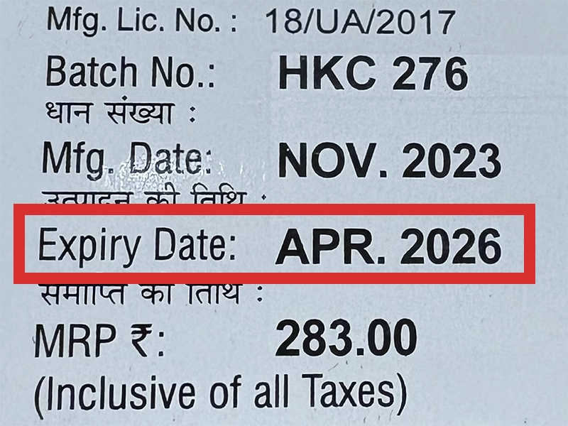
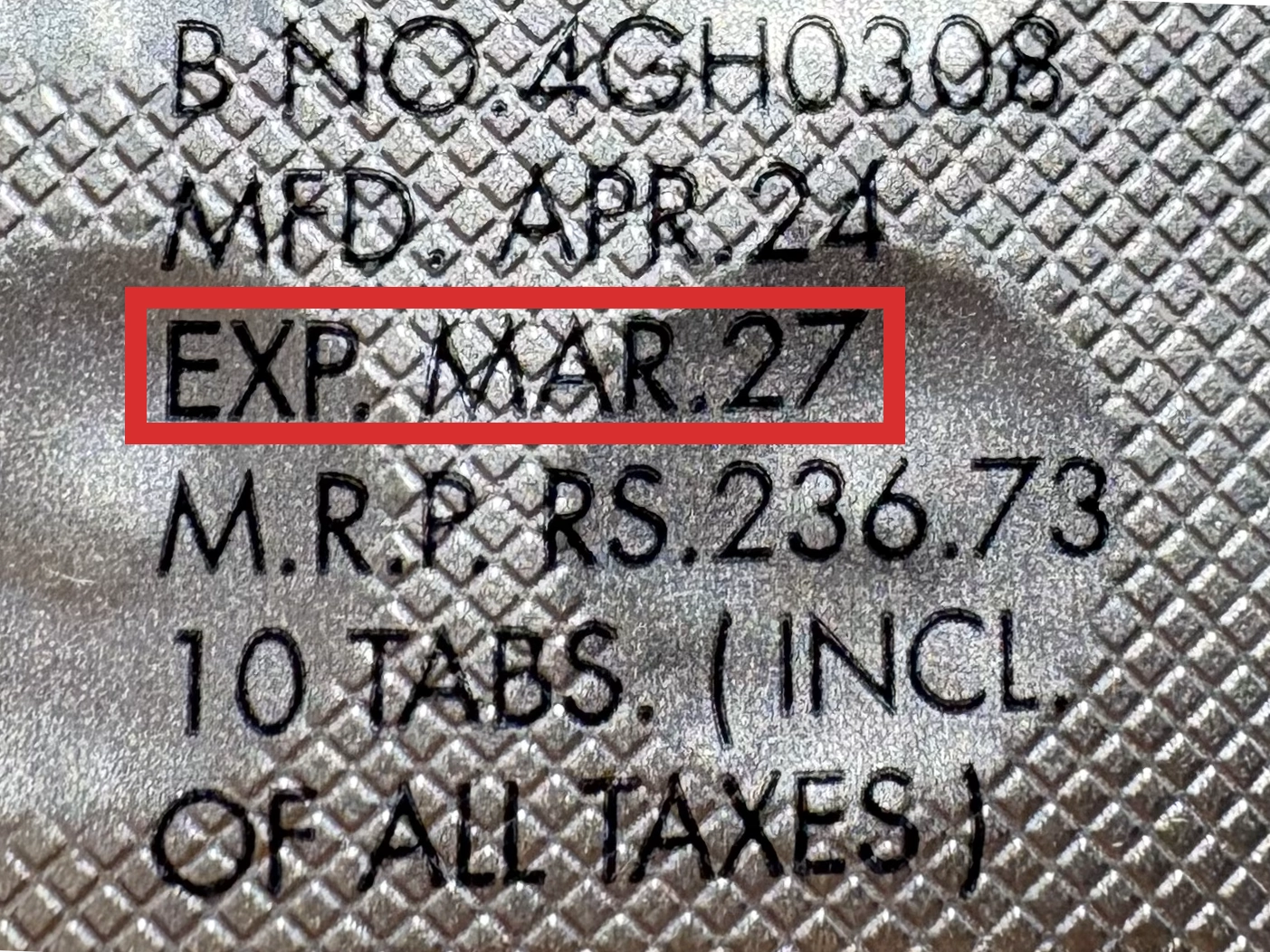
※国や製品により日付の並び(例:月/年、日/月/年)が異なる場合がありますのでご注意ください
EXP(Expiry Date) の表記がなく、MFG または MFDしか記載がないケースがあります。
この場合は MFG(MFD) から2~3年が使用期限の目安です。
※「LOT」や「BATCH」の表記は製造番号であり期限ではありません。

パッケージ例となります。
商品やご注文単位によってはシート単位でのお届けとなる場合が御座います。
外箱に当サイト名や商品名が記載されることはないため、ご家族や配達員など第三者に内容を知られることは御座いません。
心臓に圧迫感のある痛みというか苦しさを感じてコンコールを使ってみました。今までに経験したことのないような痛みと場所が場所なだけにかなり焦りました。焦ると余計に痛くなるような気がしたのでできるだけ自分を落ち着かせるためにも薬は有効的でした。今ではほとんど痛くなることがなくなったので薬の回数を減らしたり痛いときにだけ飲むようにして副作用の影響を減らしています!
昔から心拍数が高く、50手前からは血圧の高さも気になっていました。不整脈もセットで顔を出し始めて、病院に行ったところメインテートとノルバスクを処方されました。効果としては血圧・不整脈ともに安定していました。病院に通うことがなかなか難しくなったときにノルバスクの代わりにコンコールを飲み始めましたが数値や症状は悪化していません。
高血圧が気になりだしてからコンコールを飲んでいますが1年経っても問題なく過ごせています。薬の効果としては上が120、下が70弱をキープしています。ジェネリックの商品よりも効果が安定しているように思え、高血圧だったことを忘れていることもあります。飲む量は半錠で安定しています。頻脈の方にも効果があるようなので気になっている人は試してみても良いと思います。
2度目のリピートになります。1度目同様到着までは10日かかりました。メインテートを服用していましたが血圧を下げると同時に頻脈にも効果が出ているので体にあっているのだと思います。コンコールに変えてからのほうが不安もなく生活できているので感謝しています。通院時間を気にしている人の常備薬として同じ症状の人におすすめしたい商品です。またリピートしたいと思います。
不整脈が出てしまい、病院に行って薬を処方してもらっていたのですが昼間の通院は難しいものがあり悩んでいたところでコンコールの話を聞いてネットで探してみました。初めてのことなので不安でしたが今の所副作用も出ておらず飲み続けています。症状は今の所緩和されているのでしっかりとした効果が出ているのだと思います。他のジェネリックも機会があれば試したいと思います。
商品口コミの投稿は会員のみ行えるようになっております。
お手数ですが会員ログインの上でご投稿頂きますようお願いいたします。
口コミをご投稿頂いたお客様にはポイントをプレゼントさせて頂いております。
文章のみであれば100ポイント、文章+写真付きのものは300ポイントをプレゼントさせて頂きます。
規約や詳細などはこちらをご確認くださいませ。