


年1の検診でメタボといわれ続けて数年なにもしてこなかったのでついに糖尿病。なんとかしてダイエットしないと本当にヤバイと言われて通院していましたが、仕事しながら通院はかなりきつくて継続できそうにない状態だったのでリピトールには本当に助けられています。ちゃんとお医者さんにも話をして(めちゃくちゃ嫌そうな顔されたけど)、指導されたダイエットも実践して今は何とかなっています。

左記クレジットカード、銀行振込、コンビニ決済に対応
左記クレジットカード、銀行振込、コンビニ決済に対応


更新日:2025/6/4
リピトールは、脂質異常症の治療薬として病院でも処方される医薬品です。
有効成分(アトルバスタチンカルシウム水和物)の働きによって悪玉コレステロールの生成を効果的に防ぎ、中性脂肪を減少させます。
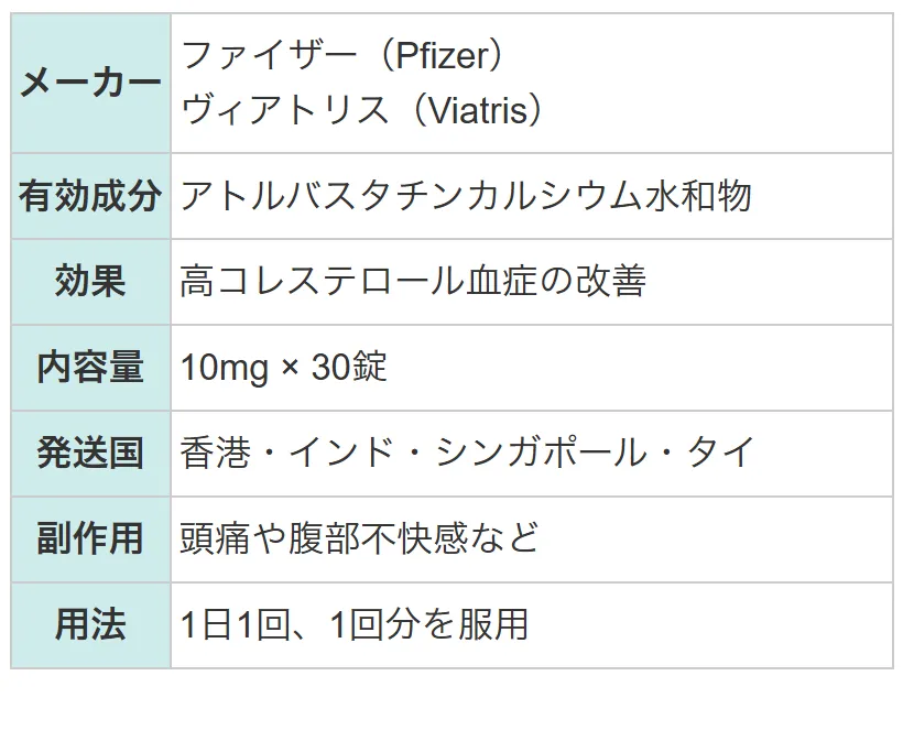
| メーカー | ファイザー(Pfizer) ヴィアトリス(Viatris) |
|---|---|
| 有効成分 | アトルバスタチンカルシウム水和物 |
| 効果 | 高コレステロール血症の改善 |
| 副作用 | 頭痛や腹部不快感など |
| 用法 | 1日1回、1回分を服用 |
アトルバスタチンカルシウム水和物は、HMG-CoA還元酵素阻害薬に分類される有効成分です。コレステロール生成に関わるHMG-CoA還元酵素の働きをブロックすることで、効果を発揮します。
リピトールには、配合量の異なる10mg錠、20mg錠、40mg錠、80mg錠の4種類があります。

| 個数 | 販売価格(1錠あたり) | 販売価格(箱) | ポイント | 購入 |
|---|---|---|---|---|
| 30錠 | 172円 | 5,160円 | 154pt |
| 個数 | 販売価格(1錠あたり) | 販売価格(箱) | ポイント | 購入 |
|---|---|---|---|---|
| 30錠 | 208円 | 6,260円 | 187pt |
| 個数 | 販売価格(1錠あたり) | 販売価格(箱) | ポイント | 購入 |
|---|---|---|---|---|
| 30錠 | 292円 | 8,760円 | 262pt |
| 個数 | 販売価格(1錠あたり) | 販売価格(箱) | ポイント | 購入 |
|---|---|---|---|---|
| 30錠 | 338円 | 10,160円 | 304pt | 売り切れ |


①1万円以上で送料無料
1回の注文で10,000円以上だった場合、1,000円の送料が無料となります。
まとめ買いをすると1商品あたりのコストパフォーマンスが高くなるためおすすめです。
②プライバシー守る安心梱包
外箱に当サイト名や商品名が記載されることはないため、ご家族や配達員など第三者に内容を知られることは御座いません。

③100%メーカー正規品取り扱い
当サイトの商品は100%メーカー正規品となっており、第三者機関による鑑定も行っております。
商品の破損などがあった場合は再配送などにて対応させて頂きますので、ご連絡頂ければ幸いです。

④いつでも購入可能 処方箋不要
サイト上では24時間いつでもご注文を受けております。
また、お電話によるご注文も受け付けておりますのでネットが苦手な方はお気軽にどうぞ。

⑤商品到着100%
商品発送後はお荷物の追跡状況が分かる追跡番号をご案内させて頂きます。
郵便局には保管期限がありますのでご注意ください。
・自宅配達で不在だった場合の保管期限・・・16日間前後
・郵便局留めとした場合の保管期限・・・7~30日間

⑥コンビニ決済利用可能
ご近所のコンビニにていつでもお支払可能です。
セブンイレブンに限り店舗での機械操作を必要とせず、手続き完了後に表示されるバーコードや払込票番号をレジに提示することでお支払い頂けます。

リピトール 10mg x 30錠
5,160円
ポイント:154pt
10,000円以上購入で送料無料
在庫あり

年1の検診でメタボといわれ続けて数年なにもしてこなかったのでついに糖尿病。なんとかしてダイエットしないと本当にヤバイと言われて通院していましたが、仕事しながら通院はかなりきつくて継続できそうにない状態だったのでリピトールには本当に助けられています。ちゃんとお医者さんにも話をして(めちゃくちゃ嫌そうな顔されたけど)、指導されたダイエットも実践して今は何とかなっています。
コレステロール値がひどいので、なんとか薬で抑え込みたくて対策を考え始めました。その一環でリピトールを買ってました。自分は体が頑丈な方だし、副作用は大丈夫だと信じていました。でも、飲めば飲むほど体がかゆくなり、病院で診てもらったらリピトールの影響でした。こんな形で副作用が出ると思ってませんでした。服用は中断させられ、今後は地道に治療を進めることになりそうです。
肝臓でコレステロールを作る酵素の働きを抑えることで、血液中の悪玉コレステロール(LDL)を減らします。さらに、肝臓のコレステロール処理機能を活性化し、余分な脂質を排出することで、コレステロールの全体量を調整するはたらきがあります。
リピトールは、同じ種類の薬であるプラバスタチンと比べてコレステロールを下げる効果が高く、少ない量でもしっかりとした効果が得られます。肝肝臓での代謝や体内での吸収効率が良いため、治療効果の安定性にも優れています。
血中の悪玉コレステロールを下げることで、動脈に脂質がたまるのを防ぎ、動脈硬化の進行を抑える効果があります。血管を健康に保つための予防薬としても使われています。
リピトールは悪玉コレステロールだけでなく、中性脂肪の値も改善する効果があります。血中脂質全体のバランスを整えることが期待できる薬です。
リピトールは、通常1日1回10mgの服用が基本です。症状や体質に応じて20mgまたは40mgまで増やすこともあります。
リピトールは1日1回で効果が持続するため、朝でも夜でも服用可能です。ただし、毎日決まった時間に飲むことで効果を安定させやすいため、生活リズムに合わせた時間帯に設定するのが理想です。
食後でなくても問題はありません。食後に飲むと吸収速度がやや遅くなることがありますが、吸収される量には大きな違いはなく、食事の影響をあまり受けないためです。
コレステロールの値が正常になっても、体質的に高くなりやすい人は服用を続けることが大切です。中断すると再び値が上昇することがあるため、医師の判断で継続が勧められます。
ごくまれに筋肉が壊れて腎臓に負担をかける横紋筋融解症が報告されています。筋肉痛や脱力感、茶色い尿などが現れたときは、すぐに服用を中止し医療機関を受診する必要があります。
一部の抗真菌薬や免疫抑制剤、C型肝炎治療薬と併用すると、血中濃度が異常に高まり、重い副作用が起こることがあります。グレカプレビルやピブレンタスビルとの併用は禁忌となっています。
まれに肝炎や黄疸など、肝機能に関わる副作用が出ることがあります。悪心や倦怠感、食欲不振などが続く場合は、肝機能障害のサインである可能性があるため注意が必要です。
消化不良、下痢、頭痛、関節痛などの軽い症状がみられることがあります。多くは一時的なもので自然に改善します。しかし、いつまでも症状が改善しないような場合には医療機関を受診するようにしましょう。
| 1日の服用回数 | 1回 |
|---|---|
| 1回の服用量 | 10mg |
| 服用のタイミング | 指定なし |
| 服用期間 | 24時間 |
| 1日の服用回数 | 1回 |
|---|---|
| 1回の服用量 | 10mg |
| 服用のタイミング | 指定なし |
| 服用期間 | 24時間 |
| 商品名 | リピトール | ピバスタ | エゼンチア | リパンシール | バイトリン | リピダトール |
|---|---|---|---|---|---|---|
| 商品画像 | |  |  |  |  |  |
| 特徴1 | 病院でも処方される脂質異常症治療薬 | ・コレステロールを抑える | ・相互作用を起こしにくい | ・中性脂肪を効果的に減少 | ・国内承認された2つの有効成分配合 | ・心筋梗塞の予防や改善に対して特に効果的 |
| 特徴2 | 悪玉コレステロールを効果的に減少させる | ・高コレステロール血症を改善する | ・コレステロール低下で動脈硬化を予防 | ・動脈硬化による様々な病気を予防 | ・1日1回の服用でコレステロールを効果的に下げる | ・世界的に使用されているリピトールのジェネリック |
| 内容量 | 10mgx30錠 | 100錠x1箱 | 10mg30錠x1箱 | 200mg30錠x1箱 | 10mg+10mg30錠x1箱 | 5mg30錠x1箱 |
| 価格 | 5,160円 | 6,460円 | 4,860円 | 6,460円 | 6,360円 | 3,860円 |
| 5%以上 | 0.1〜5%未満 | 頻度不明 | |
| 皮膚 | そう痒感、発疹、皮疹、発赤 | 脱毛症、光線過敏、皮膚乾燥、皮膚亀裂、爪の障害 | |
| 血液 | 血小板減少、白血球減少、貧血 | ||
| 肝臓 | AST上昇、ALT上昇、γ-GTP上昇 | Al-P上昇、LDH上昇、肝障害 | |
| 消化器 | アミラーゼ上昇、嘔吐、下痢、胃炎、軟便、嘔気、口内炎、胸やけ、便秘、胃不快感、腹痛、心窩部痛(心窩部の疼痛)、腹部膨満感 | 膵炎、胆汁うっ滞性黄疸、食欲不振、消化不良、悪心、口渇、舌痛、舌炎、舌のしびれ、口のしびれ、口唇炎、咽頭不快感 | |
| 呼吸器 | 咳 | ||
| 筋骨格系 | CK上昇 | 痙攣、筋炎、筋肉痛、血中ミオグロビン上昇、無力症、関節痛、頸・肩のこり、胸痛、背部痛、こわばり感、腱炎、腱痛 | |
| 感覚器 | 異常感覚、末梢神経障害、耳鳴、霧視 | ||
| 精神神経系 | めまい、不眠(症) | 勃起障害、四肢しびれ(感)、眠気、健忘症、抑うつ、悪夢 | |
| 内分泌 | テストステロン低下 | コリンエステラーゼ上昇、TSH上昇、ACTH上昇、アルドステロン低下 | 女性化乳房 |
| 代謝異常 | グルコース上昇、HbA1c上昇、血清鉄低下 | 低血糖症 | |
| 腎臓 | K上昇 | BUN上昇、血中クレアチニン増加、血尿 | |
| その他 | 脳梗塞、肺炎、頭痛、全身倦怠(感)、帯状疱疹 | 浮腫(顔面・四肢等)、動悸、頻脈、味覚異常、頻尿、排尿困難、着色尿、熱感、発熱 |
本製品は海外製のため、期限表記が日本と異なる場合がございます。
パッケージ裏面や側面、シートなどに以下のような表記がされています。
| EXP | 使用期限 例:EXP 12/2025→2025年12月まで使用可 |
|---|---|
| MFG または MFD | 製造日 例:MFG 03/2023 |
| BEST BEFORE | 品質が最も安定している目安日 |
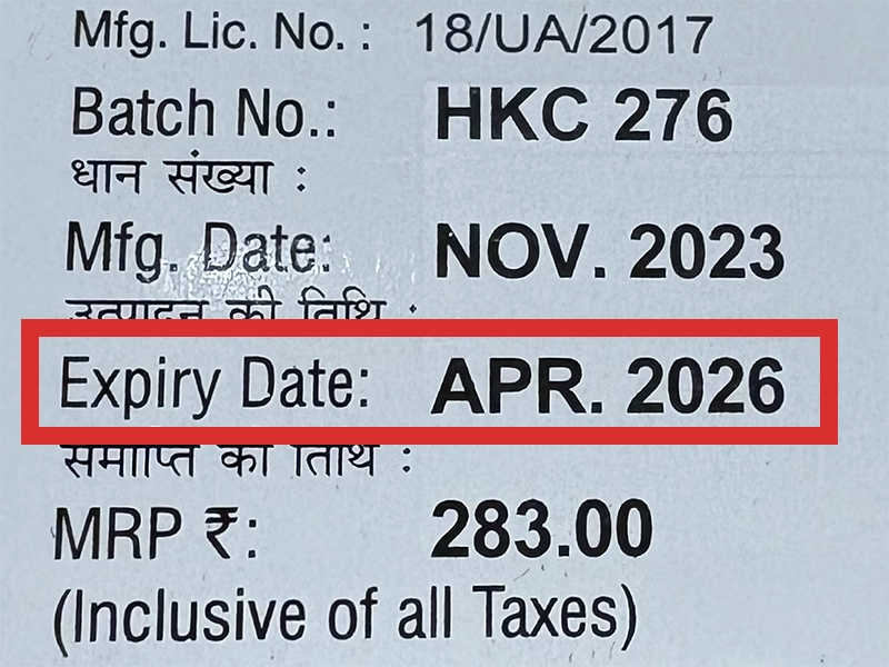
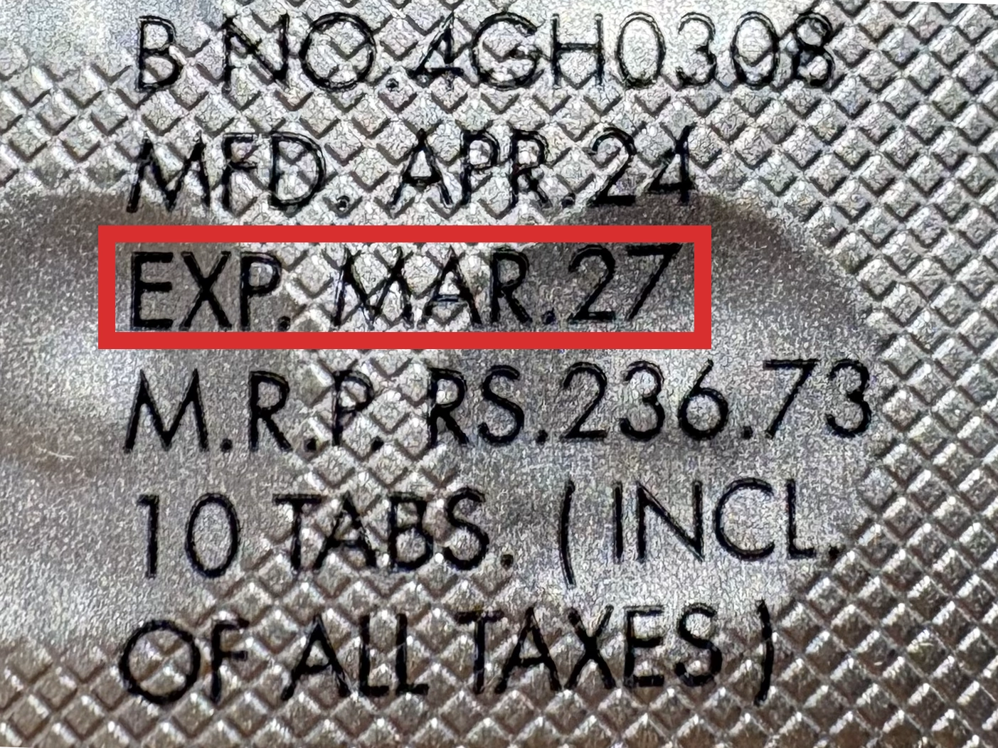
※国や製品により日付の並び(例:月/年、日/月/年)が異なる場合がありますのでご注意ください
EXP(Expiry Date) の表記がなく、MFG または MFDしか記載がないケースがあります。
この場合は MFG(MFD) から2~3年が使用期限の目安です。
※「LOT」や「BATCH」の表記は製造番号であり期限ではありません。

パッケージ例となります。
商品やご注文単位によってはシート単位でのお届けとなる場合が御座います。
外箱に当サイト名や商品名が記載されることはないため、ご家族や配達員など第三者に内容を知られることは御座いません。
年1の検診でメタボといわれ続けて数年なにもしてこなかったのでついに糖尿病。なんとかしてダイエットしないと本当にヤバイと言われて通院していましたが、仕事しながら通院はかなりきつくて継続できそうにない状態だったのでリピトールには本当に助けられています。ちゃんとお医者さんにも話をして(めちゃくちゃ嫌そうな顔されたけど)、指導されたダイエットも実践して今は何とかなっています。
まだ使用したてなので特に効果の実感的なところはできていません。少しやせてきたかな?とかそれくらいは感じるんですけど、まだまだこれからですかね。頑張ります。
ダイエット成功しました。製薬会社がPfizerってあったので安心して買えました。中性脂肪の数値がかなり悪かったのですが、中性脂肪落とすためにはどうすればいいのか全く分からなくてとにかく我武者羅にダイエットをし続けてきたんですが、それでも中性脂肪が減らずで苦労しました。リピトールを使いだしてからはしっかり改善することができました!中性脂肪の数値も今のところ落ちてきています。175から160になっただけなのでまだまだ高いのは変わらないんですけど、今後も使い続けてなんとか正常値に戻したいなと思っています。
会社の健康診断で高コレステロール血症の診断を受けてから使い始めてます。使い始めてから2ヶ月程度になりますが、今はコレステロール値も下がって安定しているので、今後も続けるか病院の先生と相談して決めたいと思ってます。使い始めは特に何も気にせず使ってましたが、食事とか運動まで考えるようにするとかなり良い感じに下がってきたのでいいですね。
高コレステロール血症の治療で処方されてる薬と同じなので購入してみました。最近は仕事の方が忙しくて病院に足を運ぶ余裕もあまりなかったんですが、こちらであれば通院せずに購入できるので非常に助かっていますね。肝心の効果についても200近くあったLDLコレステロール値もこれを使い始めてから徐々に落ちてきてもうすこしで正常範囲で落ち着きそうなのでかなり良い感じです。
商品口コミの投稿は会員のみ行えるようになっております。
お手数ですが会員ログインの上でご投稿頂きますようお願いいたします。
口コミをご投稿頂いたお客様にはポイントをプレゼントさせて頂いております。
文章のみであれば100ポイント、文章+写真付きのものは300ポイントをプレゼントさせて頂きます。
規約や詳細などはこちらをご確認くださいませ。