使い始めてから大体5週間ほどで、飲み始める前よりも筋肉がついてきたなと変化を実感できました!久々に会った友達からもなんか逞しくなった?と言われたので、気のせいじゃないと思います!試しに飲んでみて正解でした!!

左記クレジットカード、銀行振込、コンビニ決済に対応
左記クレジットカード、銀行振込、コンビニ決済に対応

更新日:2025/6/5
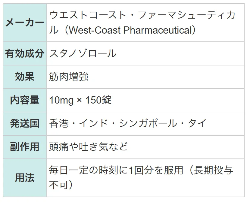
ウィンゾロンは、1959年に開発されたアナボリックステロイド(タンパク質同化ステロイド)のスタノゾロールを有効成分とする筋肉増強剤です。
海外では現役の医薬品(適応症:低身長症など)でもあり、長い歴史と実績があります。
| メーカー | ウエストコースト・ファーマシューティカル(West-Coast Pharmaceutical) |
|---|---|
| 有効成分 | スタノゾロール |
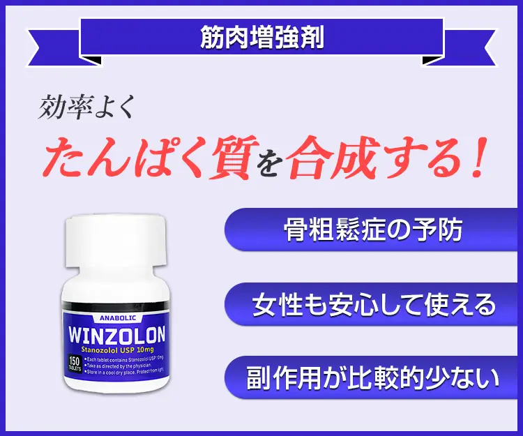
| 効果 | 筋肉増強 |
| 副作用 | 頭痛や吐き気など |
| 用法 | 毎日一定の時刻に1回分を服用(長期投与不可) |
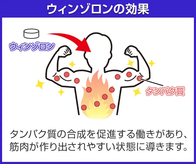
スタノゾロールは、男性ホルモンに類似した構造を持つ有効成分です。アンドロゲン(男性ホルモン)受容体に作用することでタンパク質合成が促進され、筋肉増強効果を発揮します。
ウィンゾロンには、1錠あたり10mgのスタノゾロールが含有されています。

| 個数 | 販売価格(1錠あたり) | 販売価格(箱) | ポイント | 購入 |
|---|---|---|---|---|
| 150錠 | 40円 | 6,060円 | 181pt | |
| 300錠 | 29円 | 8,760円 | 262pt |


①1万円以上で送料無料
1回の注文で10,000円以上だった場合、1,000円の送料が無料となります。
まとめ買いをすると1商品あたりのコストパフォーマンスが高くなるためおすすめです。
②プライバシー守る安心梱包
外箱に当サイト名や商品名が記載されることはないため、ご家族や配達員など第三者に内容を知られることは御座いません。

③100%メーカー正規品取り扱い
当サイトの商品は100%メーカー正規品となっており、第三者機関による鑑定も行っております。
商品の破損などがあった場合は再配送などにて対応させて頂きますので、ご連絡頂ければ幸いです。

④いつでも購入可能 処方箋不要
サイト上では24時間いつでもご注文を受けております。
また、お電話によるご注文も受け付けておりますのでネットが苦手な方はお気軽にどうぞ。

⑤商品到着100%
商品発送後はお荷物の追跡状況が分かる追跡番号をご案内させて頂きます。
郵便局には保管期限がありますのでご注意ください。
・自宅配達で不在だった場合の保管期限・・・16日間前後
・郵便局留めとした場合の保管期限・・・7~30日間

⑥コンビニ決済利用可能
ご近所のコンビニにていつでもお支払可能です。
セブンイレブンに限り店舗での機械操作を必要とせず、手続き完了後に表示されるバーコードや払込票番号をレジに提示することでお支払い頂けます。

ウィンゾロン 10mg x 150錠
6,060円
ポイント:181pt
10,000円以上購入で送料無料
在庫あり

使い始めてから大体5週間ほどで、飲み始める前よりも筋肉がついてきたなと変化を実感できました!久々に会った友達からもなんか逞しくなった?と言われたので、気のせいじゃないと思います!試しに飲んでみて正解でした!!
自力で筋トレをするより短期間で効率よく筋肉をつけられるのは認める。だが、ニキビができやすくなり、ひどいときは吐くこともある。健康的に筋肉量を増やすのには向いてない。
アナボリックステロイドを服用することによって、テストステロンの分泌が減少してしまいます。その結果、精子の産生が減少してしまいます。精子の産生が減少してしまうことで子供ができる確率は下がってしまいます。ただし、完全にゼロとなってしまうわけではないため、子作りは不可能ではありません。
アナボリックステロイドの効果については、配合成分によって作用のアプローチにも違いがあるためです。ダイエット向きとされるものの成分は水分の貯留であったり、副作用が少ないといったことが挙げられています。こうしたことから、目的に合わせて使用するものを選ぶのも有効です。
アナボリックステロイドの使用を辞めることは可能です。ただし、その場合、ステロイドによって筋肥大がステロイド未使用の限界をこえているような状態を維持することはできません。そのため、ステロイドを使用せずにトレーニングしている状態をこえた筋肉量を維持したいと考えている場合には継続しての使用などが必要になります。
アナボリックステロイドの錠剤と注射で効果に違いはありません。筋力量の増加を促進することで、筋肥大などに期待することが可能となっています。
アナボリックステロイドは蛋白同化作用を持っているため、効果的な筋力増強を可能にします。一方でプロテインは栄養素であるタンパク質を効率的に補う健康食品であるため、プロテインそのものに筋力増強の作用はありません。そのため、筋力増強の効果という点で考えると、アナボリックステロイドの方が効果があると言えます。
| 1日の服用回数 | 1~2回 |
|---|---|
| 1回の服用量 | 25~100mg |
| 服用のタイミング | 朝食後もしくは朝晩の食後 |
| 服用間隔 | 12~24時間 |
| 商品名 | スタノゾロール | アナドリン | メダナボル | オキシポロン | ハロフルオックス | プリモノロン | アンドロフォルテクリーム | テストステロンジェル |
|---|---|---|---|---|---|---|---|---|
| 商品画像 |  |  |  |  |  |  |  |  |
| 特徴1 | 筋肉や骨を強くする有効成分を配合 | ・骨髄の機能を高める効果にも期待できる | 効率よく筋肉増強をサポートする | ・骨髄の機能を高める効果にも期待できる | ・体脂肪を減らす効果にも期待できる | ・女性化作用や肝臓への負担が少ない | ・手軽に男性ホルモンを補給できる | 男性ホルモン補充で筋肉増強 |
| 特徴2 | 造血力UPにより貧血改善にも期待できる | ・カルシウムの排出量を抑えて骨を強化する | ボトル1本にたっぷり60錠入り | ・トレーニングのサポートにも最適 | ・服用を中止しても一定期間、効果が持続する | ・従来の筋肉増強剤より安全性が高い | ・さっと使用することができる外用薬タイプ | 皮膚から直接有効成分を取り込めるクリーム |
| 内容量 | 2mgx20錠 | 10mgx60錠 | 10mgx60錠 | 50mgx60錠 | 5mgx120錠 | 25mgx150錠 | 5%x1箱 | 1% 5gx1本 |
| 価格 | 2,760円 | 6,260円 | 4,360円 | 5,860円 | 14,060円 | 29,160円 | 24,460円 | 1,800円 |
本製品は海外製のため、期限表記が日本と異なる場合がございます。
パッケージ裏面や側面、シートなどに以下のような表記がされています。
| EXP | 使用期限 例:EXP 12/2025→2025年12月まで使用可 |
|---|---|
| MFG または MFD | 製造日 例:MFG 03/2023 |
| BEST BEFORE | 品質が最も安定している目安日 |
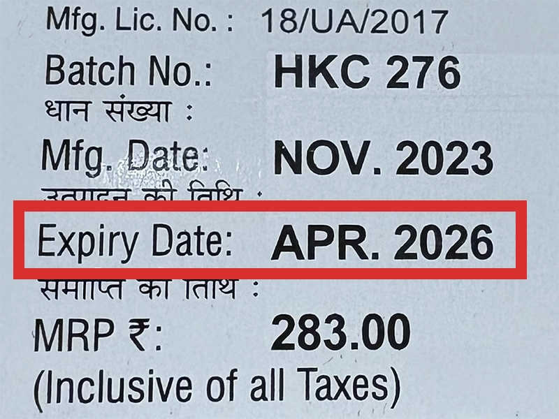
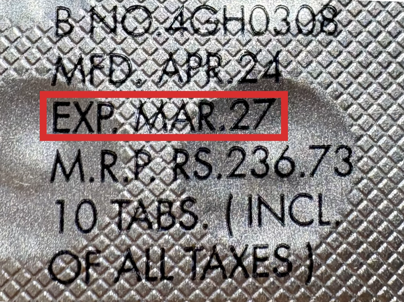
※国や製品により日付の並び(例:月/年、日/月/年)が異なる場合がありますのでご注意ください
EXP(Expiry Date) の表記がなく、MFG または MFDしか記載がないケースがあります。
この場合は MFG(MFD) から2~3年が使用期限の目安です。
※「LOT」や「BATCH」の表記は製造番号であり期限ではありません。

パッケージ例となります。
商品やご注文単位によってはシート単位でのお届けとなる場合が御座います。
外箱に当サイト名や商品名が記載されることはないため、ご家族や配達員など第三者に内容を知られることは御座いません。
使い始めてから大体5週間ほどで、飲み始める前よりも筋肉がついてきたなと変化を実感できました!久々に会った友達からもなんか逞しくなった?と言われたので、気のせいじゃないと思います!試しに飲んでみて正解でした!!
パンプアップしているような感覚があり、しっかりとトレーニングに励むことができます。飲むのと飲まないのとでは大違いなので、効率よく筋力アップしたいときは使うのをおすすめします。副作用の話もちらほら聞きますが、自分はあまり気になりませんでした。もうすぐ飲みきってしまいそうなので、また追加で何箱か購入させていただきます。
筋肉の増加が停滞していましたがこれはかなり効ます、停滞していた時間が一気に加速し進むかのような感じです。二頭筋が一回り大きくなりました、久しく忘れていた成長という感動を思い出しました。継続という言葉を思い出させてくれてありがとうございます。
この薬を飲むようになりかなり好調です!筋肉が喜んでいるのがわかります!300錠で買うとお得なのも良いですね!この調子で筋肉を育んでいきます!追加注文したので発送のほどよろしくお願いします。
市販のプロテインだと効果を実感できなかったので、仲間内で噂になっているこちらを購入することにしました。現在飲み始めて1ヶ月半ほどですが、なかなか育ってきてる感じがしています、しっかり継続していこうと考えています。
商品口コミの投稿は会員のみ行えるようになっております。
お手数ですが会員ログインの上でご投稿頂きますようお願いいたします。
口コミをご投稿頂いたお客様にはポイントをプレゼントさせて頂いております。
文章のみであれば100ポイント、文章+写真付きのものは300ポイントをプレゼントさせて頂きます。
規約や詳細などはこちらをご確認くださいませ。