


ネットでケアプロストが良いって見てから気になってて、使ってみたら・・・スカスカまつ毛がフサフサまつ毛になりました!はじめはコツがいるけど慣れたら一瞬で塗れちゃいます♪

左記クレジットカード、銀行振込、コンビニ決済に対応
左記クレジットカード、銀行振込、コンビニ決済に対応

更新日:2025/6/18
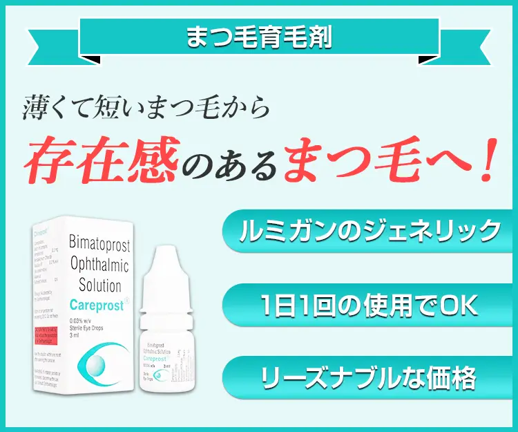
ケアプロストは、緑内障治療薬・まつ毛育毛薬として高い実績を誇るビマトプロストを有効成分とする医薬品です。
1日1回1滴をまつ毛に垂らすだけで育毛効果を発揮するほか、1日1回1滴を眼球に垂らすだけで緑内障の治療を進めることができます。
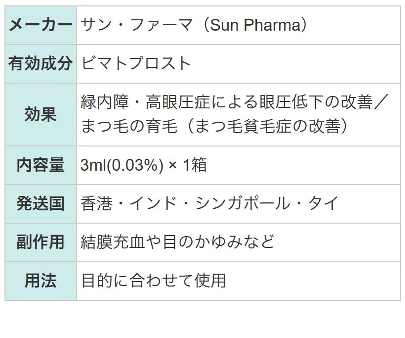
| メーカー | サン・ファーマ(Sun Pharma) |
|---|---|
| 有効成分 | ビマトプロスト |
| 効果 | 緑内障・高眼圧症による眼圧低下の改善/まつ毛の育毛(まつ毛貧毛症の改善) |
| 副作用 | 結膜充血や目のかゆみなど |
| 用法 | 目的に合わせて使用 |
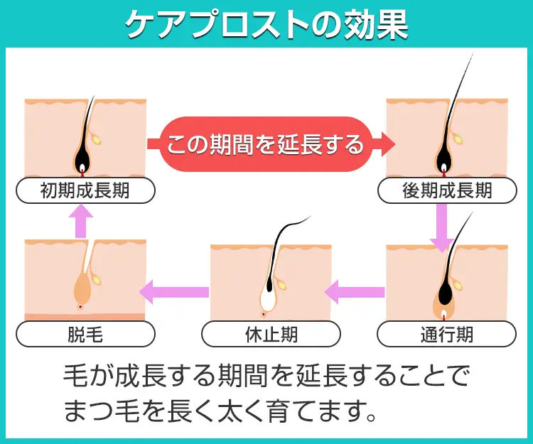
ビマトプロストは、まつ毛の毛包に作用することで育毛を進める作用があります。細胞分裂を促進し、育毛サイクルにおける成長期を伸ばすことで、自然に長いまつ毛を実現します。また、眼球に作用して眼圧を下げ、緑内障を改善する効果もあります。
ケアプロスト3mlに、ビマトプロスト0.03%が含有されています。

| 個数 | 販売価格(1箱あたり) | 販売価格(箱) | ポイント | 購入 |
|---|---|---|---|---|
| 1箱 | 3,560円 | 3,560円 | 106pt | |
| 3箱 | 3,386円 | 10,160円 | 304pt | |
| 5箱 | 3,232円 | 16,160円 | 484pt |


①1万円以上で送料無料
1回の注文で10,000円以上だった場合、1,000円の送料が無料となります。
まとめ買いをすると1商品あたりのコストパフォーマンスが高くなるためおすすめです。
②プライバシー守る安心梱包
外箱に当サイト名や商品名が記載されることはないため、ご家族や配達員など第三者に内容を知られることは御座いません。

③100%メーカー正規品取り扱い
当サイトの商品は100%メーカー正規品となっており、第三者機関による鑑定も行っております。
商品の破損などがあった場合は再配送などにて対応させて頂きますので、ご連絡頂ければ幸いです。

④いつでも購入可能 処方箋不要
サイト上では24時間いつでもご注文を受けております。
また、お電話によるご注文も受け付けておりますのでネットが苦手な方はお気軽にどうぞ。

⑤商品到着100%
商品発送後はお荷物の追跡状況が分かる追跡番号をご案内させて頂きます。
郵便局には保管期限がありますのでご注意ください。
・自宅配達で不在だった場合の保管期限・・・16日間前後
・郵便局留めとした場合の保管期限・・・7~30日間

⑥コンビニ決済利用可能
ご近所のコンビニにていつでもお支払可能です。
セブンイレブンに限り店舗での機械操作を必要とせず、手続き完了後に表示されるバーコードや払込票番号をレジに提示することでお支払い頂けます。

ケアプロスト 3ml(0.03%) x 1箱
3,560円
ポイント:106pt
10,000円以上購入で送料無料
在庫あり

ネットでケアプロストが良いって見てから気になってて、使ってみたら・・・スカスカまつ毛がフサフサまつ毛になりました!はじめはコツがいるけど慣れたら一瞬で塗れちゃいます♪
いつも使ってるまつ毛美容液よりも高いけど、気になってたから買ってみた。でも、期待しすぎたかもな~思ってたよりも伸びないし、太さも変わらない。
ビマトプロストは睫毛の「長さ」「太さ」「色の濃さ」の3点に明確な改善効果を示します。臨床試験では、使用4か月後に約77〜89%の被験者で「際立ち度」が向上し、まつ毛の長さや密度が有意に増加したことが示されています。
4か月使用後、まつ毛の平均的な長さは1.6mm以上増加し、見た目にも明らかな変化が報告されています。なお、使用をやめると元の状態に戻る可能性があります。
がん化学療法後の睫毛貧毛症に対しても88.9%の被験者で改善が認められています。ケアプロストを用いた治療開始は化学療法終了から4週間以降が推奨されます。抗がん剤による辛い状態を改善できるため、QOLの向上にも繋がります。
ケアプロストは睫毛貧毛症の治療薬として承認されており、眉毛への有効性は確認されていません。そのため、効果については明確には確認されていません。
まつ毛育毛の場合、上まつ毛の根元にアプリケーターを使って塗布します。そのため、目薬のように点眼して使うことはありません。間違った使い方をしてしまうと効果を得られないどころか、副作用の危険もあるため注意してください。
下まつ毛には使用しないことが定められています。これはビマトプロストが上まつ毛専用であるためです。皮膚への色素沈着などの副作用を避けるためにも、指定部位以外への塗布は控えてください。
効果の向上は確認されていません。1日2回以上の使用は過剰な使用となってしまうため、副作用のリスクが高まってしまう可能性があります。そのため、適切な用法用量を守って使用するようにしてください。
就寝前に使用するので、メイクを落としてスキンケアを行った後に使います。清潔で乾いた状態のまぶたにのみ塗布してください。塗布後は余分な薬液をコットンなどでふき取ります。
使用を中止することはできます。ただし、使用を中止した場合は、次第に元のまつ毛の状態へと戻っていってしまいます。育毛したまつ毛を維持する場合は効果を得た後も継続して使用する必要があります。
使用することは可能です。ただし、効果などについての臨床は行われていないため、どういった効果があるのかも不明な部分が多いです。そのため、髪の毛に使うのは避けた方が良いといえます。
塗布時に上まつ毛以外に付着する可能性があります。そうした時は、すぐにふき取ってください。また、使用中に虹彩色素沈着は投与中止後も元に戻らないことがあるため、事前に説明が必要です。
結膜充血や眼瞼掻痒症、眼瞼紅斑や点状角膜炎などが報告されています。臨床試験では副作用の発現率は25.1%とされており、4人に1人程度に何らかの副作用が出る可能性があります。
| 1日の服用回数 | 1回 |
|---|---|
| 1回の服用量 | 1滴 |
| 服用のタイミング | 就寝前 |
| 服用間隔 | 24時間 |
| 商品名 | ケアプロスト+アプリケーター80本セット | ルミガン+アプリケーター60本セット | ビマトアイドロップ | ルミガン | モデルアイズ・モデラッシュ | ヒマラヤアイライナーカジャル | ケアプロストプラス | リバイタラッシュ |
|---|---|---|---|---|---|---|---|---|
| 商品画像 |  |  |  |  |  |  |  |  |
| 特徴1 | ・日本国内でも認可されている成分を配合 | ・日本国内で唯一認可されたまつ毛美容液 | 病院処方のルミガンと同一成分を配合 | 世界初の医療用まつ毛育毛成分を配合 | ・手軽にまつ毛の成長を促進できる | ・100%天然成分で作られたアイライナー | ・緑内障や高眼圧症の対策にも効果的 | ・まつ毛に保湿力と柔軟性を与える効果もある |
| 特徴2 | ・専用のアプリケーターで清潔に使用できる | ・はじめての人も使いやすいセット製品 | 1日1回1滴の使用でまつ毛が伸びる | 確かな実績があり、安心して使える | ・1本で約70日間使用することが可能 | ・敏感肌の方でも安心して使用できる | ・使用開始から約8週間で効果を実感できる | ・まつ毛の貧毛や脱毛などの症状に効果的 |
| 内容量 | 3ml(0.03%)x1セット | 3ml(0.03%)x1セット | 3ml(0.03%)x1本 | 3ml(0.01%)x1箱 | 5mlx1本 | 1GRAMx1本 | 3mlx1本 | 3.5mlx1本 |
| 価格 | 4,160円 | 5,460円 | 3,060円 | 5,960円 | 3,860円 | 2,660円 | 4,360円 | 19,660円 |
| 5%以上 | 1〜5%未満 | 0.1〜1%未満 | 頻度不明 | |
| 眼 | 睫毛の異常(睫毛が長く、太く、濃くなる等)(52.8%)、結膜充血(44.9%)、眼瞼色素沈着(20.5%)、眼そう痒症(9.6%)、眼瞼の多毛症 | 結膜炎、結膜浮腫、結膜出血、眼瞼浮腫、眼瞼紅斑、眼瞼そう痒症、眼瞼障害、眼脂、点状角膜炎、角膜びらん、眼刺激、霧視、眼の異常感(違和感、べとつき感等)、くぼんだ眼 | 結膜色素沈着、眼瞼炎、眼瞼下垂、霰粒腫、マイボーム腺梗塞、糸状角膜炎、角膜血管新生、虹彩炎、眼乾燥、眼の灼熱感、眼痛、羞明、白内障、眼精疲労、視力低下、視覚障害、眼球運動失調、眼圧上昇 | ぶどう膜炎、黄斑浮腫、乾性角結膜炎、流涙、涙液分泌低下 |
| 循環器 | 狭心症発作、高血圧 | |||
| 消化器 | 胃不快感 | |||
| 呼吸器 | 咳嗽 | |||
| その他 | 尿潜血、CK増加 | 口唇疱疹、浮動性めまい、頭痛、胸痛、耳鳴、白血球数増加、ALT(GPT)増加、γ−GTP増加 |
本製品は海外製のため、期限表記が日本と異なる場合がございます。
パッケージ裏面や側面、シートなどに以下のような表記がされています。
| EXP | 使用期限 例:EXP 12/2025→2025年12月まで使用可 |
|---|---|
| MFG または MFD | 製造日 例:MFG 03/2023 |
| BEST BEFORE | 品質が最も安定している目安日 |
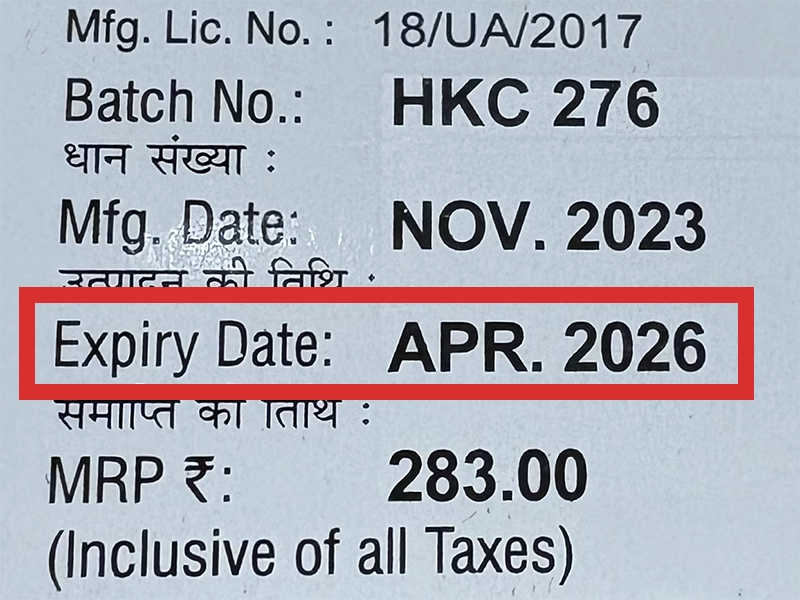
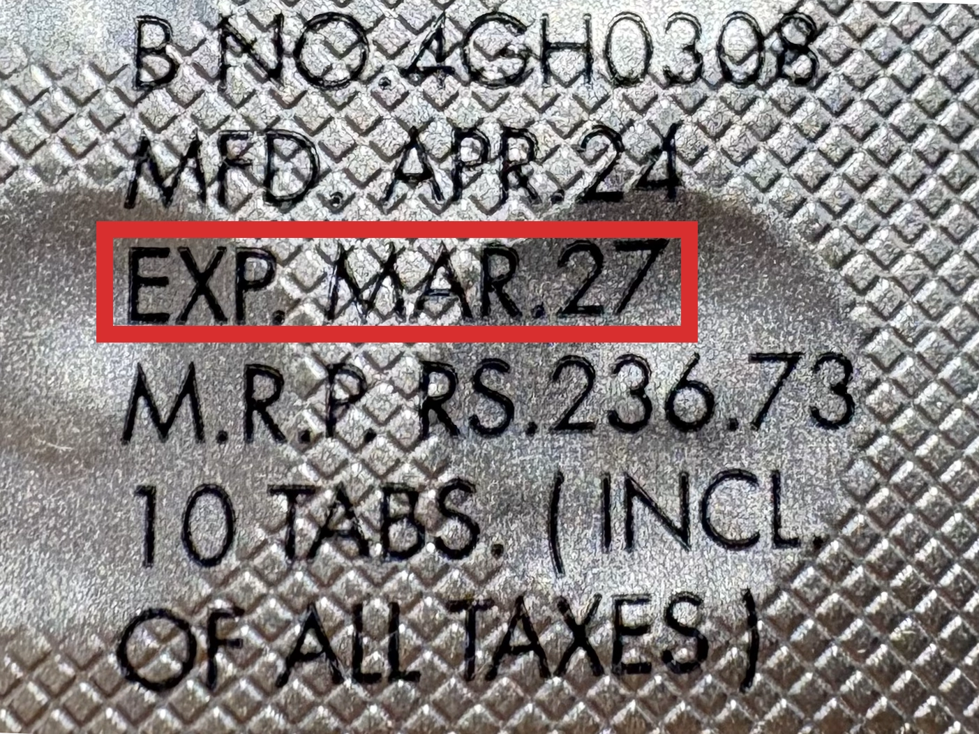
※国や製品により日付の並び(例:月/年、日/月/年)が異なる場合がありますのでご注意ください
EXP(Expiry Date) の表記がなく、MFG または MFDしか記載がないケースがあります。
この場合は MFG(MFD) から2~3年が使用期限の目安です。
※「LOT」や「BATCH」の表記は製造番号であり期限ではありません。

パッケージ例となります。
商品やご注文単位によってはシート単位でのお届けとなる場合が御座います。
外箱に当サイト名や商品名が記載されることはないため、ご家族や配達員など第三者に内容を知られることは御座いません。
まつ毛は増えた感じはするけど、長さは変わってません。量より長さがほしいんですけど~~~!もっと続ければ長くなる?ねぇ教えて?ww
マツエクしてる?ってくらいまつ毛が長い子がいて、聞いてみたらこれを使ってるって言ってたので使ってるけど全然伸びません。。1本使って変化なければやめます。
ネットでケアプロストが良いって見てから気になってて、使ってみたら・・・スカスカまつ毛がフサフサまつ毛になりました!はじめはコツがいるけど慣れたら一瞬で塗れちゃいます♪
ライターで右まつ毛を燃やしてしまい緊急で購入しました。二週間ほど商品到着までかかったけど買って良かったなと思える商品です。一週間程度で育毛効果を実感できました。
ツケマで傷んだまつ毛の修復目的で購入しました。細いまつ毛が少しずつ太く強くなっているので使い切った時が楽しみです。リピはそこから考えます。
商品口コミの投稿は会員のみ行えるようになっております。
お手数ですが会員ログインの上でご投稿頂きますようお願いいたします。
口コミをご投稿頂いたお客様にはポイントをプレゼントさせて頂いております。
文章のみであれば100ポイント、文章+写真付きのものは300ポイントをプレゼントさせて頂きます。
規約や詳細などはこちらをご確認くださいませ。